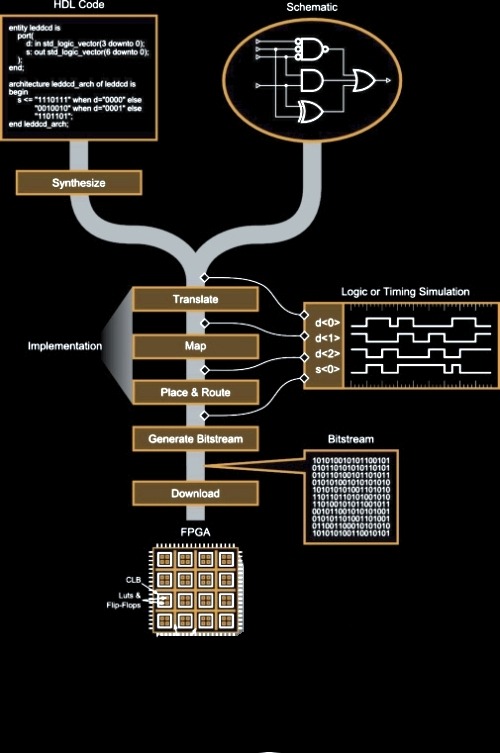
In this part of tutorial we are going to have a short intro on FPGA design flow. A simplified version of FPGA design flow is given in the flowing diagram.

Design Entry
There are different techniques for design entry. Schematic based, Hardware Description Language and combination of both etc. . Selection of a method depends on the design and designer. If the designer wants to deal more with Hardware, then Schematic entry is the better choice. When the design is complex or the designer thinks the design in an algorithmic way then HDL is the better choice. Language based entry is faster but lag in performance and density.
HDLs represent a level of abstraction that can isolate the designers from the details of the hardware implementation. Schematic based entry gives designers much more visibility into the hardware. It is the better choice for those who are hardware oriented. Another method but rarely used is state-machines. It is the better choice for the designers who think the design as a series of states. But the tools for state machine entry are limited. In this documentation we are going to deal with the HDL based design entry.
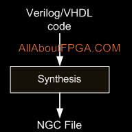
Synthesis
The process which translates VHDL or Verilog code into a device netlist formate. i.e a complete circuit with logical elements( gates, flip flops, etc…) for the design.If the design contains more than one sub designs, ex. to implement a processor, we need a CPU as one design element and RAM as another and so on, then the synthesis process generates netlist for each design element
Synthesis process will check code syntax and analyze the hierarchy of the design which ensures that the design is optimized for the design architecture, the designer has selected. The resulting netlist(s) is saved to an NGC( Native Generic Circuit) file (for Xilinx® Synthesis Technology (XST)).
Implementation
This process consists a sequence of three steps
1. Translate
2. Map
3. Place and Route
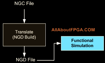
Translate process combines all the input netlists and constraints to a logic design file. This information is saved as a NGD (Native Generic Database) file. This can be done using NGD Build program. Here, defining constraints is nothing but, assigning the ports in the design to the physical elements (ex. pins, switches, buttons etc) of the targeted device and specifying time requirements of the design. This information is stored in a file named UCF (User Constraints File).
Tools used to create or modify the UCF are PACE, Constraint Editor etc.
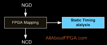
Map process divides the whole circuit with logical elements into sub blocks such that they can be fit into the FPGA logic blocks. That means map process fits the logic defined by the NGD file into the targeted FPGA elements (Combinational Logic Blocks (CLB), Input Output Blocks (IOB)) and generates an NCD (Native Circuit Description) file which physically represents the design mapped to the components of FPGA. MAP program is used for this purpose.
Place and Route PAR program is used for this process. The place and route process places the sub blocks from the map process into logic blocks according to the constraints and connects the logic blocks. Ex. if a sub block is placed in a logic block which is very near to IO pin, then it may save the time but it may effect some other constraint. So trade off between all the constraints is taken account by the place and route process
The PAR tool takes the mapped NCD file as input and produces a completely routed NCD file as output. Output NCD file consists the routing information.
Device Programming
Now the design must be loaded on the FPGA. But the design must be converted to a format so that the FPGA can accept it. BITGEN program deals with the conversion. The routed NCD file is then given to the BITGEN program to generate a bit stream (a .BIT file) which can be used to configure the target FPGA device. This can be done using a cable. Selection of cable depends on the design.
Design Verification
Verification can be done at different stages of the process steps.
Behavioral Simulation (RTL Simulation) This is first of all simulation steps; those are encountered throughout the hierarchy of the design flow. This simulation is performed before synthesis process to verify RTL (behavioral) code and to confirm that the design is functioning as intended. Behavioral simulation can be performed on either VHDL or Verilog designs. In this process, signals and variables are observed, procedures and functions are traced and breakpoints are set. This is a very fast simulation and so allows the designer to change the HDL code if the required functionality is not met with in a short time period. Since the design is not yet synthesized to gate level, timing and resource usage properties are still unknown.
Functional simulation(Post Translate Simulation) Functional simulation gives information about the logic operation of the circuit. Designer can verify the functionality of the design using this process after the Translate process. If the functionality is not as expected, then the designer has to made changes in the code and again follow the design flow steps.
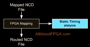
Static Timing Analysis This can be done after MAP or PAR processes Post MAP timing report lists signal path delays of the design derived from the design logic. Post Place and Route timing report incorporates timing delay information to provide a comprehensive timing summary of the design.