Table of Contents
Introduction
![]()
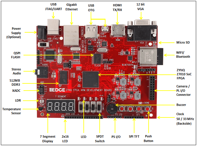
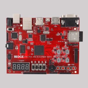
EDGE ZYNQ SoC FPGA Development Board is a feature rich and high-performance Single Board Computer built around the Xilinx Zynq-7000 (XC7Z010 or XC7Z020). It features integrated dual-core ARM Cortex-A9 processor with Xilinx 7-series FPGA.
EDGE ZYNQ SoC FPGA Development Board is designed to create best learning experience of both processing system (PS) and programming logic (PL). It features Xilinx XC7Z010 or XC7Z020 SoC, 512MB DDR3 SDRAM and 16MB QSPI Flash USB-to-UART, USB OTG, 10/100/1000Mbps Ethernet, HDMI, USB JTAG, Temperature sensor, Micro SD, WiFi, Bluetooth, ADC, LCD, 7 Segment, camera, TFT, Buzzer, Switches, buttons and LEDs.
Advantage of EDGE FPGA kit is easy to implement plenty of applications ranging from single board computer, Wireless control, Image/video Processing, Internet of Things without additional interfaces.
Xilinx offers free WebPACK™ versions of Vivado design suite, so designs can be implemented at no additional cost.
Board Applications
• Single Board Computer
• Wireless control
• Environment monitor
• IoT (Internet of Things)
• Image Processing
• Video Processing
• Audio Processing
Board Features
• Xilinx Zynq XC7Z010-1CLG400C or XC7Z020-1CLG400C FPGA
• 512MB DDR3
• 16MB QSPI Flash
• On-Board USB JTAG Programmer
• USB to UART Interface
• 10/100/1000M Ethernet
• USB OTG
• Micro SD
• WiFi 802.11 b/g/n
• Bluetooth 4.2 and BLE
• 12 bit VGA Interface
• HDMI Tx/Rx
• ADC 2 channel
• Temperature Sensor
• LDR Interface
• Stereo Audio Jack
• 2×16 LCD Display
• 4 Digit Seven Segment Display
• 50 MHz and 33 MHz Clock
• 4 Slide switches
• 2 PL and 1 PS Push Button
• 5v Buzzer
• 4 PL and 1 PS LED
• 31 PL and 4 PS I/O
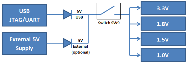
Power Supply
EDGE ZYNQ FPGA development board can get 5V power from USB JTAG Port U21. If additional power required for your application, connect 5V DC at connector J16. Now both power from USB Port and External Power supply combined and supplied to the board. Switch SW9 can be used to turn ON/OFF the power to the board.
Board consist of 4 Voltage regulators 3.3v, 1.8v, 1.5v and 1v. The Kit requires 3.3v supply for FPGA I/O and board peripherals. The 1.8v Voltage is for FPGA Auxiliary supply and ADC. The 1.5v is required DDR3 Memory. The 1v power supply is dedicated for FPGA Core and Block RAM voltage.
Caution: Only 5v Supply must be connected to the board.
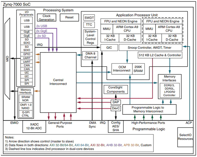
ZYNQ All Programmable SoC Architecture
The development board uses Xilinx’s Zynq7000 series chip, XC7Z010-1CLG400C. Zynq architecture is divided in to processor system (PS) and programmable logic (PL).
The PS system integrates two ARM CortexTM-A9 processors, AMBA® interconnects, internal memory, external memory interfaces, and peripherals. These peripherals mainly include USB bus interface, Ethernet interface, SD/SDIO interface, I2C bus interface, CAN bus interface, UART interface, GPIO and so on. The PS can operate independently and start on power-up or reset. The overall block diagram of the ZYNQ7000 chip is shown in Figure.
The PL is nearly identical to a Xilinx 7-series Artix FPGA, except that it contains several dedicated ports and buses that tightly couple it to the PS. The PL also does not contain the same configuration hardware as a typical 7-series FPGA, and it must be configured either directly by the processor or via the JTAG port.
ZYNQ Configuration
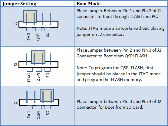
EDGE ZYNQ FPGA development board supports 3 boot modes. The three boot modes are JTAG, QSPI FLASH and SD card mode. After the ZYNQ chip is powered on, it will detect the level of the responding MIO port to determine which boot mode. Users can select different boot modes through the J2 jumper on the board. The boot mode is configured at the J2 connector as shown in Table
QSPI FLASH
EDGE ZYNQ Board features a 4-bit SPI (quad-SPI) serial NOR flash. The Multi-I/O SPI Flash memory is used to provide non-volatile boot, application code, and data storage. It can be used to initialize the PS subsystem as well as configure the PL subsystem (bitstream).
Spansion QSPI FLASH is 128Mbit, x1, x2, and x4 support and Speeds up to 104 MHz, supporting Zynq configuration rates @ 100 MHz. In Quad-SPI mode, this translates to 400Mbs.
The SPI Flash connects to the Zynq PS QSPI interface. This requires connection to specific pins in MIO Bank 0/500, specifically MIO[1:6]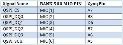
MicroSD Card
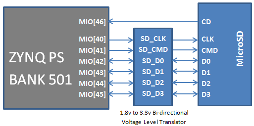
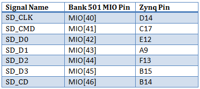
The EDGE ZYNQ board provides a microSD slot (U4) for non-volatile external memory storage as well as booting the Zynq. The slot is wired to Bank 1/501 MIO[40-47], including Card Detect. On the PS side peripheral SDIO 0 is mapped out to these pins and controls communication with the SD card. The pinout can be seen in Table 4. The peripheral controller supports 1-bit and 4-bit SD transfer modes, but does not support SPI mode. Based on the Zynq TRM, SDIO host mode is the only mode supported.
Both low speed and high speed cards are supported, the maximum clock frequency being 50 MHz. A Class 4 card or better is recommended.
DDR3 Memory
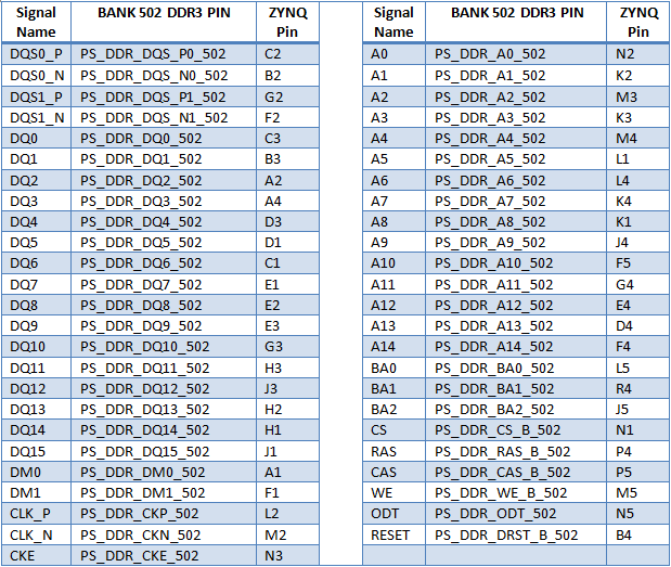
The EDGE ZYNQ development board is equipped with micron 4Gbit (512MB) DDR3 SDRAM, MT41K256M16RA-125. The DDR bus width is 16 bits. The maximum operating speed of DDR3 SDRAM is up to 533MHz (data rate 1066Mbps). The DDR3 memory system is directly connected to the memory interface of the BANK 502 of the ZYNQ processing system (PS).
Both the memory chips and the PS DDR bank are powered from the 1.5V supply. The mid-point reference of 0.75V is created with a simple resistor divider and is available to the Zynq as external reference.
USB 2.0
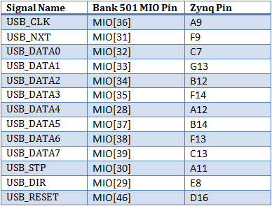
The USB 2.0 transceiver used by the EDGE ZYNQ is a 1.8V, high-speed USB3320C-EZK that supports the ULPI standard interface. ZYNQ’s USB bus interface is connected to the USB3320C-EZK transceiver to enable high-speed USB2.0 Host and Slave mode data communications.
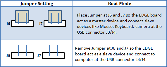
The data and control signals of the USB3320C USB are connected to the IO port of the BANK501 on the PS side of the ZYNQ chip. A 24 MHz crystal provides the system clock to the USB3320C. The development board provides users with two USB ports, one is the Host USB port and the other is the Slave USB port. They are USB Type A and Micro USB, which allow users to connect different USB peripherals. Users can switch between Host and Slave through J5 and J6 jumpers on the development board. Table shows the mode switching instructions:
The USB OTG interface can act as an embedded host or a peripheral device. The USB mode is controlled from software by manipulating the USB0 peripheral controller in the Zynq.
Gigabit Ethernet
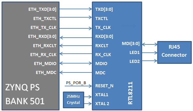
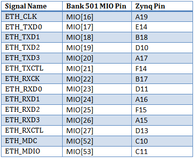
The EDGE board uses a Realtek RTL8211E-VL PHY to implement a 10/100/1000 Ethernet port for network connection. The PHY connects to MIO Bank 501 (1.8V) and interfaces to the Zynq-7000 AP SoC via RGMII for data and MDIO for management. The auxiliary interrupt (INTB) and reset (PHYRSTB) signals connect to PL pins to be accessed via EMIO. The connection diagram can be seen on Figure. After power-up the PHY starts with Auto Negotiation enabled, advertising 10/100/1000 link speeds and full duplex. If there is an Ethernet-capable partner connected, the PHY automatically establishes a link with it, even with the Zynq not configured.
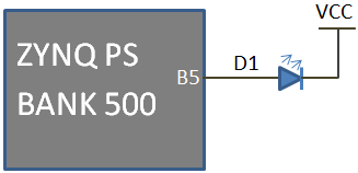
PS LED
On the EDGE development board, 1 LED is connected to the BANK500 IO of the PS section. Users can use this LED to debug the program. When the BANK500 IO voltage is high, the LED light goes out, and when the BANK500 IO voltage is low, the LED is lit. The block diagram of the connection between the ZYNQ BANK500 IO and the LED is shown in Figure.
![]()
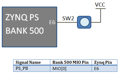
PS Push Button
On the EDGE development board, 1 push button is connected to the BANK500 IO of the PS section. The user can use this push buttons to test the input signal and interrupt trigger. When the button is pressed in the design, the signal voltage input to the ZYNQ BANK500 IO is low, and when it is not pressed, the signal is high. A block diagram of the ZYNQ BANK501 IO and key connections is shown in Figure.
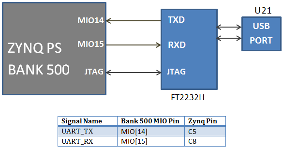
USB UART
EDGE board implements a USB-to-UART bridge connected to a PS UART peripheral. A FTDI FT2232H USB-to-UART Bridge device allows connection to a host computer. The FT2232H connects to the USB Type B connector, J2. Only basic TXD/RXD connection is implemented.
FTDI chip consist of 2 channels for JTAG and UART Communication. Once the programming is done though USB JTAG, the same USB port act as a USB UART communication.
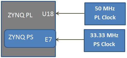
Clock – PS and PL
The EDGE ZYNQ board contains 33.33 MHz Oscillator at the ZYNQ PS Side to provide clock input to the Processing system and 50 MHz Oscillator at the FPGA PL side. The PL input clock can drive MMCMs or PLL to generate clocks of various frequencies and with known phase relationships that may be needed throughout a design.
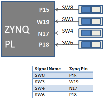
Slide Switches
The EDGE board includes 4 SPDT slide switches for digital input. These digital inputs are connected to ZYNQ FPGA through resistors for protection against short circuit. Slide switch outputs constant high or constant low based on the user changing its position.
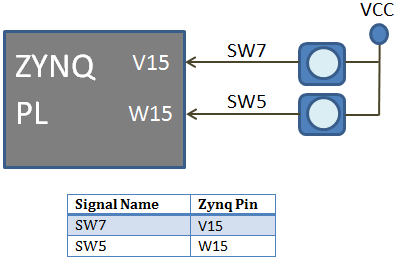
Push Buttons
The EDGE Board contains 2 Push buttons for providing momentary digital inputs at ZYNQ PL. They are connected to FPGA lines through resistors to prevent short circuit. By default the switch is in Active low. When the user pressed the push button they are driven high.
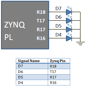
LEDs
The Kit consists of 16 LEDs for displaying digital outputs. These LED’s are connected with FPGA through a series resistor. Logic High signal turns ON LED and Logic Low signal turns OFF LED to demonstrate the digital output.
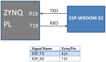
WIFI/Bluetooth/BLE
The EDGE Board contains On-board ESP-WROOM-32 WIFI/Bluetooth/BLE Module connected with ZYNQ FPGA through serial interface. When ESP Module acts as a WIFI Modem, it helps to communicate FPGA with cloud. The Data can be stored and retrieved from the cloud with the help of AT Commands. The range of communication for WIFI modem is 50 – 100 meter distance.
When ESP32 Module act as a Bluetooth V4.2, Data can be transferred between EDGE board and Bluetooth enabled devices.
Note: To enable power supply to the ESP-WROOM-32 Modem, place jumper at Enable and centre pin of J3. To disable power, place jumper at Disable and centre pin of J8.
J9 connector got TX, RX and GPIO0 Line of ESP32 module for testing and firmware update.
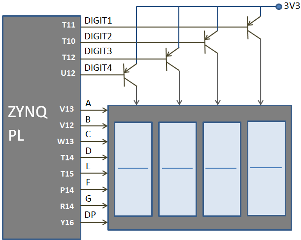
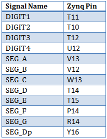
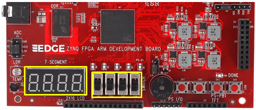
Seven segment Display
The EDGE Board consist of 4 digit 7 segment displays with common anode. Each of the seven segment contains LEDs can be turned on by sending active low signal.
For example, to display digit 8 in the seven segments display. All the segments are enabled using active low ‘0’ signal.
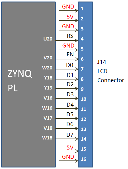
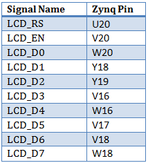
2×16 LCD
The EDGE board consist of 2×16 LCD interface at the female connector J7. LCD displays is interfaced in the 8 bit data mode, RS pin are used to select data/command mode and En are used to enable the LCD.
Note: R/W pin is connected to ground to keep LCD in always write mode.
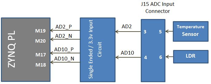
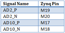
Analog Input
Pins 2 and 3 of the J15 ADC connector are used as analog inputs to the XADC module of the ZYNQ FPGA. The FPGA expects that the inputs range from 0-1 V, so we use an external circuit to scale down the input voltage from 3.3V. This circuit is shown in Figure. This circuit allows the XADC module to accurately measure any voltage between 0V and 3.3V that is applied to these pins.
The XADC core within the ZYNQ is a dual channel 12-bit analog-to-digital converter capable of operating at 1 MSPS. Either channel can be driven by any of the two auxiliary analog inputs connected to the DIP pins. The XADC core is controlled and accessed from a user design via the Dynamic Reconfiguration Port (DRP). The DRP also provides access to voltage monitors that are present on each of the FPGA’s power rails, and a temperature sensor that is internal to the FPGA. For more information on using the XADC core, refer to the Xilinx document titled 7 Series FPGAs and Zynq-7000 All Programmable SoC XADC Dual 12-Bit 1 MSPS Analog-to-Digital Converter.
External Temperature Sensor LM35 Input is available at the 5th pin of ADC Connector. To Connect Temperature sensor with XADC, Place a jumper between 3rd and 5th pin of J15 Connector. LDR input is available at the 6th pin of ADC Connector. To Connect LDR sensor with XADC, Place a jumper between 4th and 6th pin of ADC Connector.
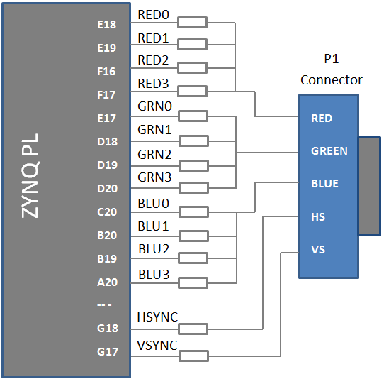
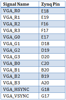
VGA
The EDGE Board contains 12 bit VGA interface to generate VGA signals from FPGA and display the output in the VGA monitor. The 12 bit VGA output the depth of 4096 colours in the Monitor. Series resistors are used to construct DAC to implement VGA interface.
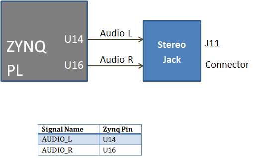
Stereo Jack
Stereo Audio Jack with low pass filter is connected on the FPGA I/O lines on the EDGE Board. Stereo Jack provides delta sigma audio output.
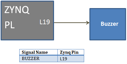
Buzzer
The Edge board contains piezo buzzer interface with FPGA through transistor. 5v Buzzer is used provide alert tone. Buzzer’s resonant frequency is 3.8 kHz (where you can expect its best performance).
Note: To enable Buzzer, place jumper at Enable and centre pin of J6. To disable power, place jumper at Disable and centre pin of J12.
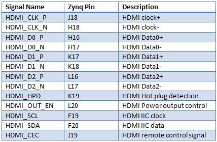
HDMI / DVI
An input and output-capable HDMI Port connects to the programmable logic pins. Over this connector an HDMI or DVI-compatible video stream can be driven in or out of the EDGE ZYNQ. Encoding or decoding the HDMI/DVI video stream needs to be implemented in logic, as well as auxiliary functions, like DDC or CEC. Depending on the actual design, it can take the Source role driving a monitor/TV display, or behave as a Sink accepting a video stream from any HDMI/DVI Source, like a laptop or smartphone.
The CEC function is bi-directional by definition, so it is treated the same no matter what role the port takes. If the CEC function is not used, declare it as input and constrain it to the correct PL pin to leave other devices on the CEC bus unaffected.
When operating as Sink, the DDC function is required to be implemented so that a connected Source can read out important characteristics of the device. This can be done by emulating an I2C-capable EEPROM in programmable logic. Likewise, in Source mode DDC can be used to find out the capabilities of the connected display.
The HDMI/DVI protocol uses TMDS (Transition-minimized differential signaling) as I/O standard. It is supported on Zynq by the I/O buffers on the programmable logic side. 50 ohm external parallel termination resistors are provided on-board. HDMI specifications only require terminations on the Sink side, but optional Source-side terminations reduce reflections, resulting in improved signal quality. Do not connect powered HDMI/DVI devices to an unpowered ZYBO, as it might result in back-powering the board through the termination resistors. Resolutions up to 720p (1280×720) have been tested.
HDMI and DVI are high-speed source-synchronous serial protocols. Implementations on FPGA are required to use certain built-in primitives to properly synthesize the correct clock frequency, serialize the transmission, and keep a lock on the signal. The actual implementation of the HDMI/DVI protocols is outside the scope of this manual. Check for upcoming reference projects on our website or consult relevant specifications and Xilinx documentation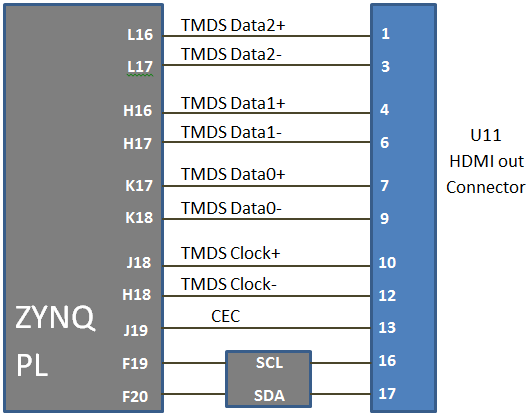
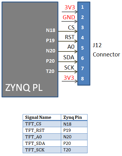
TFT Display
The EDGE Board contains TFT display interface at the J10 connector. TFT display communicates with FPGA through SPI protocol. SPI TFT is made of ST7732S SPI controller with 160×128 Display.
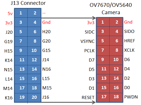
20 Pin Expansion Connector / CMOS Camera Interface
Expansion connector J13 provides 16 I/O lines from Zynq FPGA to the external interface.
Note: To interface OV7670/OV5640 CMOS Camera with EDGE Board. Leave pin1 and pin2 unconnected. Connect pin3 of expansion connector to pin1 of CMOS Camera.
Driver Installation
Vivado design Suite automatically installs drivers for EDGE ZYNQ Board. To verify it, Connect EDGE ZYNQ SoC FPGA Kit to PC through USB cable and Turn On the kit.
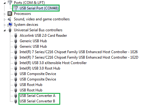
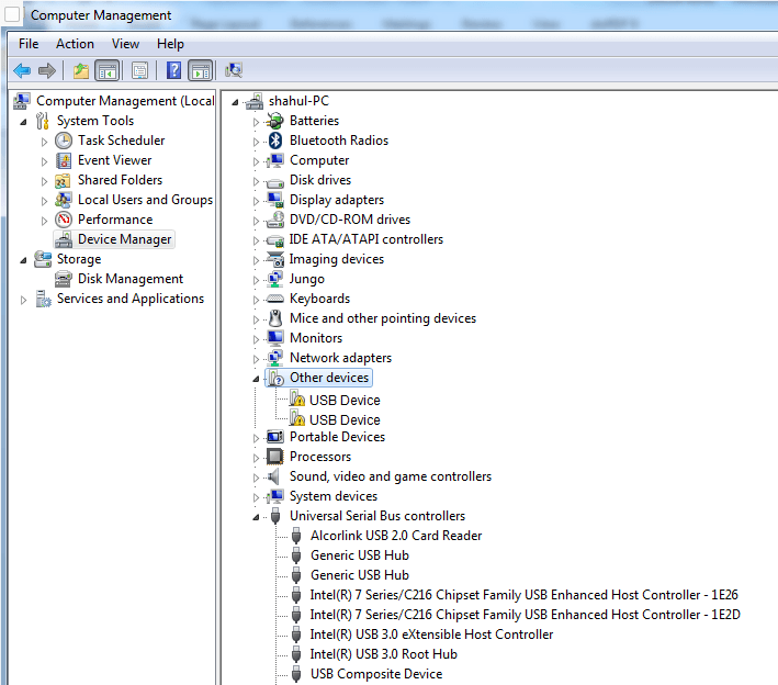
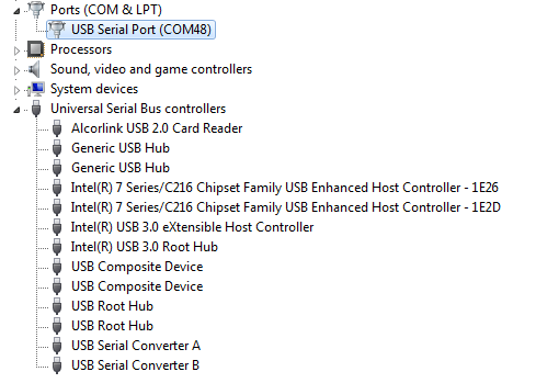
Open device manager and check the following drivers are installed. If it detecting USB Serial Port and USB Serial Converters as Shown below, then you can skip driver installation procedure and start working with Configuring FPGA using Vivado.
If the drivers are not installed, you could see the USB device under Other Devices Category as shown below. Then you have to follow the driver installation steps given below.
Step1: Download and install virtual com port USB Driver for FTDI Chip.
http://www.ftdichip.com/Drivers/VCP.htm
Step2: Install driver by right click downloaded file and run as administrator
Step3: Connect USB cable to FPGA kit U21 USB Port and another end to PC USB Port.
Step4: Open Device Manager. There are 2 other devices detected without drivers as shown in figure.
Step5: Right Click on the first USB device and select update driver.
Now select let me pick from the list of device drivers from my computer as shown below.
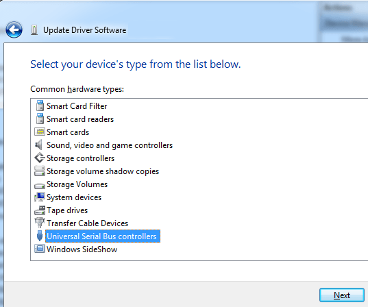
Step6: Now Select USB Serial Bus Controllers and click next.
Step7: Select FTDI under manufacturer and select USB Serial converter A under model. (If multiple driver with Serial converter A present select latest version)
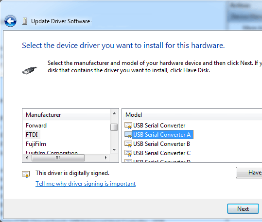
Step8: Repeat step 5 to step 7 for second unknown device. On step 7 select USB Serial Converter B instead A.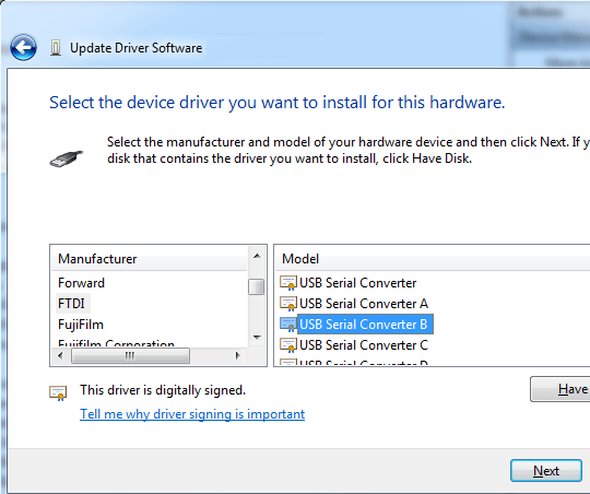
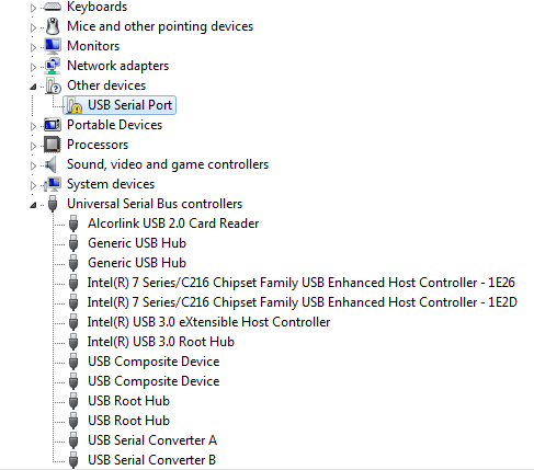
Step9: Now both USB Serial Convertor A and USB Serial Convertor B are detected under USB Controllers. But there another driver needs to be installed for USB Serial Port.
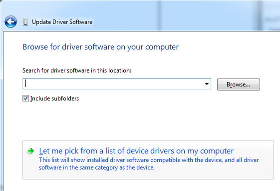
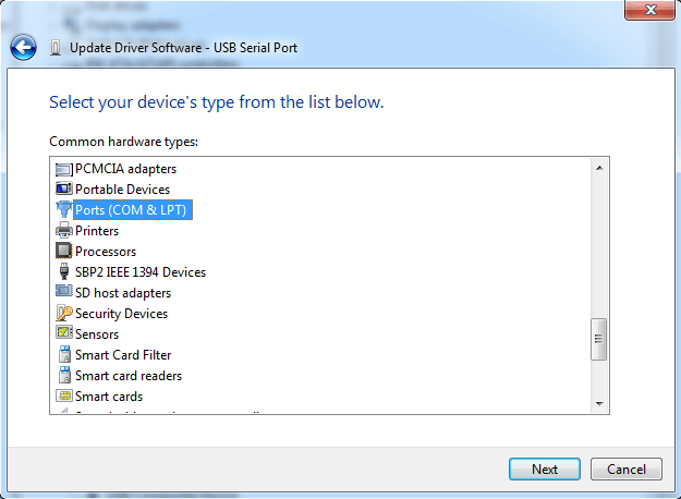
Step10: To install USB Serial Port, Right click and select update drive. Now select Browse computer for driver software and select let me pick from the list of device drivers from my computer as shown below.
Step11: Select Ports option and click next.
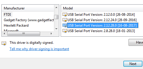
Step12: Select FTDI under manufacturer and Select USB Serial Port under Model.
Step13: Now Drivers are installed and devices are detected under Ports and USB Controllers section.
Programming EDGE Board ZYNQ FPGA using Vivado Design Suite
• Connect EDGE Zynq FPGA Kit to PC through USB cable and Turn On the kit.
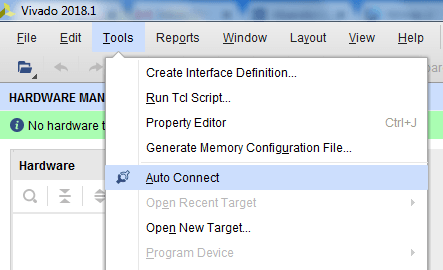
• Open “Hardware Manager -> Open Target -> Auto Connect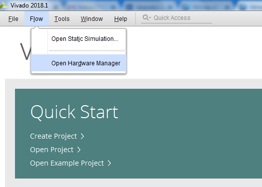
- If the device is detected successfully, then select “Program Device” by right click on the target device “xc7z010” or “xc7z020”as shown below
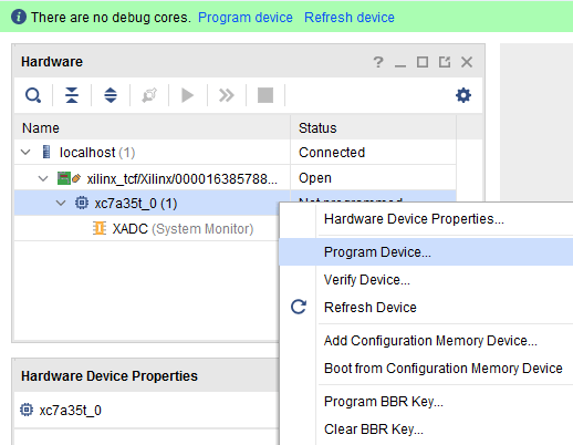
• Browse the Bit file need to be downloaded to the Zynq FPGA and click Program.
- Once the Program Succeeds, Done LED D8 light up on EDGE ZYNQ SoC FPGA kit.
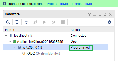
- Verify the BCD to 7 Segment output by changing switch state and see the value in display.
-
 EDGE ZYNQ SoC FPGA Development Board₹ 17,500