Table of Contents
Introduction
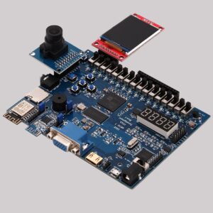
EDGE Artix 7 FPGA Development board is upgraded version of EDGE Spartan 6 board. It is exclusively designed for the latest vivado Design Suite. The EDGE Artix 7 board is built around Xilinx Artix 7 XC7A35T FPGA IC. The features includes external memory SDRAM, HDMI Out, Micro SD, WiFi, Bluetooth, ADC, DAC, LCD, 7 Segment, camera, TFT, Buzzer, Switches, buttons and LEDs interface. Real Time image and video processing can be easily implemented with 32 MB of SDRAM onboard.
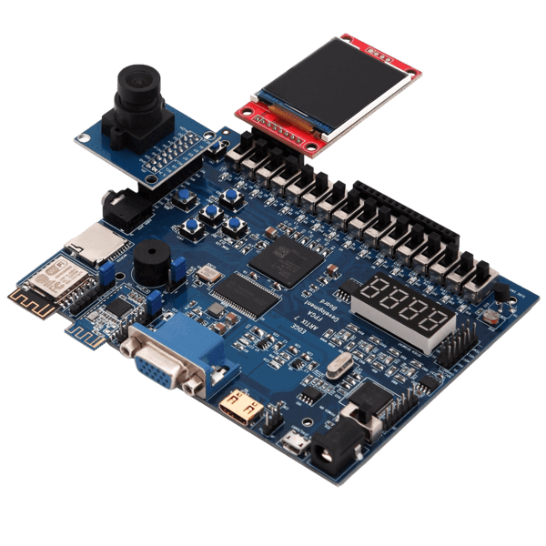
EDGE FPGA kit is ready to use Laboratory kit for ECE Curriculum. It can be useful for developing basic to advanced level digital circuits.
Advantage of EDGE FPGA kit is easy to implement plenty of applications ranging from Wireless control, Image/video Processing, Internet of Things without additional interfaces.
Xilinx offers free WebPACK™ versions of Vivado design suite, so designs can be implemented at no additional cost
Board Application
• Wireless control
• Environment monitor
• IoT (Internet of Things)
• Product Prototyping
• Image Processing
• Video Processing
• Audio Processing
Board Features
• Xilinx XC7A35T-1FTG256 Artix 7 FPGA
• 8MB SPI FLASH Memory
• 32MB SDRAM
• HDMI Out
• Micro SD Slot
• On-Board USB JTAG Programmer
• USB to UART Interface
• WIFI Interface
• Low Power Bluetooth Interface
• 12 bit VGA Interface
• 8 Channel SPI ADC
• Temperature Sensor
• LDR Interface
• SPI DAC
• 2×16 LCD Display
• 4 Digit Seven Segment Display
• 5v Buzzer
• CMOS Camera Interface
• TFT Display Interface
Power Supply
EDGE Artix 7 development board can get 5V power from either USB JTAG Port U9 or External Power Supply connector J5. Switch SW2 can be used to select the source of power from USB or External Power Supply.
Board consist of 3 Voltage regulators 3.3v, 1.8v and 1v. The Kit requires 3.3v supply for FPGA I/O, SRAM, Clock, USB, ADC, DAC, FLASH, and so on. The 1.8v Voltage is for FPGA Auxiliary supply and ADC. The 1v power supply is dedicated for FPGA Core and Block RAM voltage.
Caution: Only 5v Supply must be provided to the board either from external source or USB connector.
Programming hardware
FPGA can be configured either from USB JTAG using Xilinx Vivado software or by on-board SPI FLASH Memory.
FPGA configured through JTAG gets erased when the power supply is removed or by pressing reset button SW1.
To store the data permanently on FPGA, we have to store the configuration bit file to SPI FLASH Memory. It automatically reconfigures the FPGA after reset or Power on.
The EDGE Artix 7 FPGA Development board is fully compatible with Xilinx Vivado design suite with on-board USB JTAG Interface.
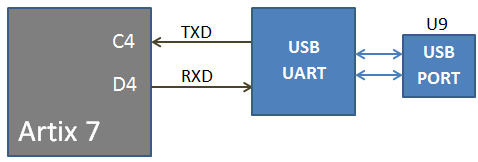
USB UART
The EDGE Board includes FT2232H IC acts as USB UART Bridge to communicate board with windows PC COM port interface.
The UART Transmitter and Receiver lines of FTDI chip is directly connected to the Artix 7 FPGA I/O pins for USB UART Communication.
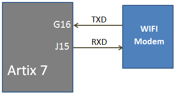
WIFI Communication
The EDGE Board contains On-board ESP8266 12F WIFI Module connected with Artix 7 FPGA through serial interface. The ESP WIFI Modem helps to communicate FPGA with cloud. The Data can be stored and retrieved from the cloud with the help of AT Commands. The range of communication for WIFI modem is 50 – 100 meter distance.
Note: To enable power supply to the WIFI Modem, place jumper at Enable and centre pin of J3. To disable power, place jumper at Disable and centre pin of J3.
J2 connector got TX, RX and GPIO0 Line of ESP12F WiFi module for testing and firmware update.
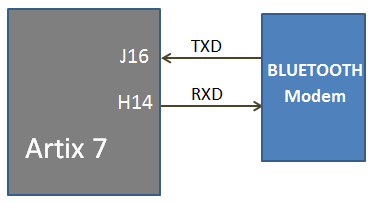
Bluetooth Communication
The EDGE contains low power Bluetooth 4.0 BLE interface on-board. The Bluetooth Module CC2541 is serially interfaced with FPGA with Transmit and Receive lines.
Note: To enable power supply to the Bluetooth Modem, place jumper at Enable and centre pin of J4. To disable power, place jumper at Disable and centre pin of J4.
J6 connector got TX, RX and Key Line of Bluetooth module for testing and firmware update.
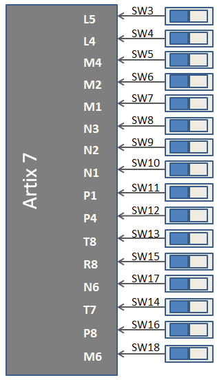
Slide Switches
The EDGE board includes 16 SPDT slide switches for digital input. These digital inputs are connected to Artix 7 FPGA through resistors for protection against short circuit. Slide switch outputs constant high or constant low based on the user changing its position.
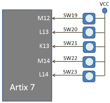
Push Buttons
The Board contains 5 Push buttons for providing momentary digital inputs. They are connected to FPGA lines through resistors to prevent short circuit. By default the switch is in Active low. When the user pressed the push button they are driven high.
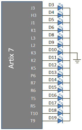
LEDs
The Kit consists of 16 LEDs for displaying digital outputs. These LED’s are connected with FPGA through a series resistor. Logic High signal turns ON LED and Logic Low signal turns OFF LED to demonstrate the digital output.
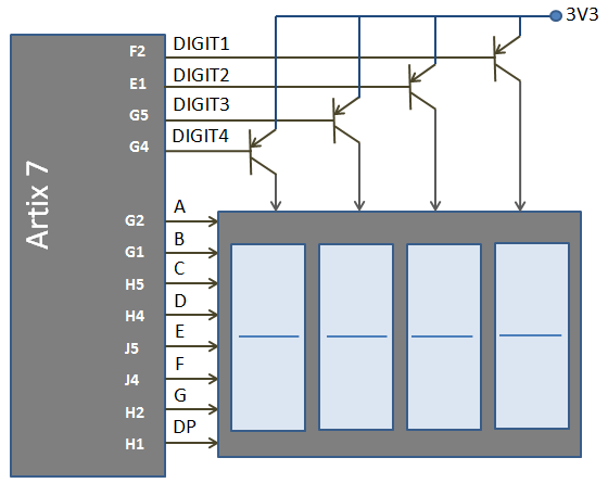
Seven segment Display
The EDGE Board consist of 4 digit 7 segment displays with common anode. Each of the seven segment contains LEDs can be turned on by sending active low signal.
For example, to display digit 8 in the seven segments display. All the segments are enabled using active low ‘0’ signal.
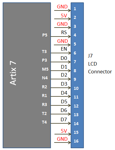
2×16 LCD
The EDGE board consist of 2×16 LCD interface at the female connector J7. LCD displays is interfaced in the 8 bit data mode, RS pin are used to select data/command mode and En are used to enable the LCD.
Note: R/W pin is connected to ground to keep LCD in always write mode.
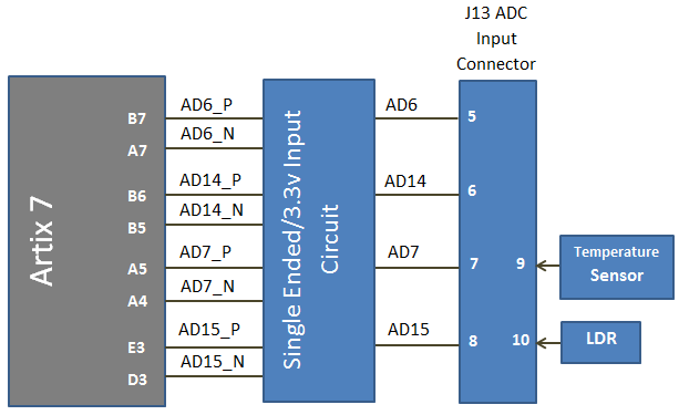
Analog Input
Pins 5, 6, 7 and 8 of the J13 ADC connector are used as analog inputs to the XADC module of the Artix 7 FPGA. The FPGA expects that the inputs range from 0-1 V, so we use an external circuit to scale down the input voltage from 3.3V. This circuit is shown in Figure. This circuit allows the XADC module to accurately measure any voltage between 0V and 3.3V that is applied to these pins.
The XADC core within the Artix-7 is a dual channel 12-bit analog-to-digital converter capable of operating at 1 MSPS. Either channel can be driven by any of the two auxiliary analog inputs connected to the DIP pins. The XADC core is controlled and accessed from a user design via the Dynamic Reconfiguration Port (DRP). The DRP also provides access to voltage monitors that are present on each of the FPGA’s power rails, and a temperature sensor that is internal to the FPGA. For more information on using the XADC core, refer to the Xilinx document titled 7 Series FPGAs and Zynq-7000 All Programmable SoC XADC Dual 12-Bit 1 MSPS Analog-to-Digital Converter.
External Temperature Sensor LM35 Input is available at the 9th pin of ADC Connector. To Connect Temperature sensor with XADC, Place a jumper between 7th and 9th pin of J13 Connector.
LDR input is available at the 10th pin of ADC Connector. To Connect LDR sensor with XADC, Place a jumper between 8th and 10th pin of ADC Connector.
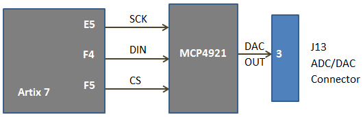
SPI DAC
The EDGE Board consist of Microchip MCP4921 SPI DAC to perform digital to analog conversion. The output is available at the male connector J13.
SPI interface provides Serial clock, Data input and chip select to FPGA with DAC. Artix 7 FPGA act as master and MCP4921 act as slave device.
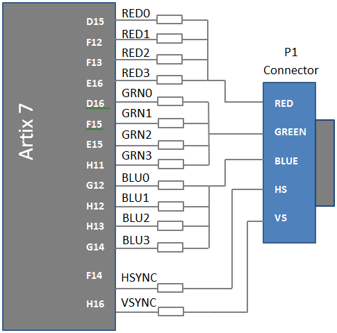
VGA
The EDGE Board contains 12 bit VGA interface to generate VGA signals from FPGA and display the output in the VGA monitor. The 12 bit VGA output the depth of 4096 colours in the Monitor. Series resistors are used to construct DAC to implement VGA interface.
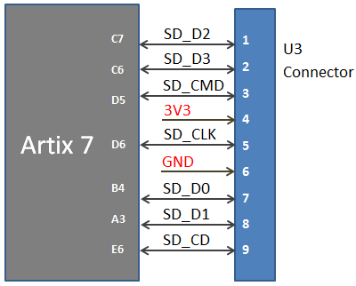
MicroSD Slot
The EDGE board provides a microSD slot (U3) for non-volatile external memory storage.
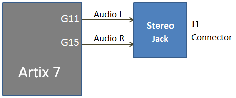
Stereo Jack
Stereo Audio Jack with low pass filter is connected on the FPGA I/O lines on the EDGE Board. Stereo Jack provides delta sigma audio output.
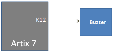
Buzzer
The Edge board contains piezo buzzer interface with FPGA through transistor. 5v Buzzer is used provide alert tone. Buzzer’s resonant frequency is 3.8 kHz (where you can expect its best performance).
Note: To enable Buzzer, place jumper at Enable and centre pin of J6. To disable power, place jumper at Disable and centre pin of J12.
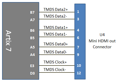
HDMI / DVI
Both HDMI and DVI systems use the same TMDS signaling standard, directly supported by Artix-7 user I/O infrastructure. Only Three differential data channels and one differential clock channel are connected with Artix 7 FPGA. Also, HDMI sources are backward compatible with DVI sinks.
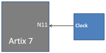
Clock
The Edge board contains 50 MHz Oscillator to provide clock input to the FPGA. The input clock can drive MMCMs or PLL to generate clocks of various frequencies and with known phase relationships that may be needed throughout a design.
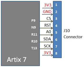
TFT Display
The EDGE Board contains TFT display interface at the J10 connector. TFT display communicates with FPGA through SPI protocol. SPI TFT is made of ST7732S SPI controller with 160×128 Display.
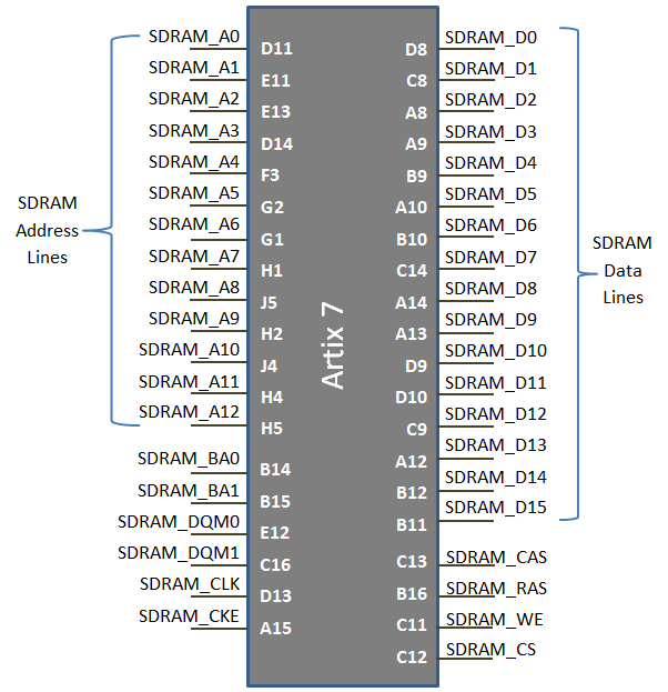
SDRAM
The EDGE Board upgraded with 32MB of SDRAM. The 32MB SDRAM is a high-speed CMOS, dynamic random-access memory containing 268,435,456 bits. It is internally configured as a quad-bank DRAM with a synchronous interface (all signals are registered on the positive edge of the clock signal, CLK). Each of the x16’s 67,108,864-bit banks is organized as 8192 rows by 512 columns by 16 bits.
Read and write accesses to the SDRAM are burst-oriented; accesses start at a selected location and continue for a programmed number of locations in a programmed sequence. Accesses begin with the registration of an ACTIVE command, which is then followed by a READ or WRITE command. The address bits registered coincident with the ACTIVE command are used to select the bank and row to be accessed (BA[1:0] select the bank; A[12:0] select the row). The address bits registered coincident with the READ or WRITE command are used to select the starting column location for the burst access.
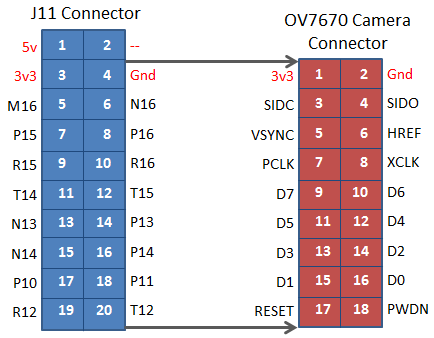
20 Pin Expansion Connector / CMOS Camera Interface
Expansion connector J11 provides 16 I/O lines from Artix 7 FPGA to the external interface.
Note: To interface OV7670 CMOS Camera with EDGE Board. Leave pin1 and pin2 unconnected. Connect pin3 of expansion connector to pin1 of CMOS Camera.
Driver Installation
Vivado design Suite automatically install drivers for EDGE Artix 7 Board. To verify it, Connect EDGE Artix 7 FPGA Kit to PC through USB cable and Turn On the kit.
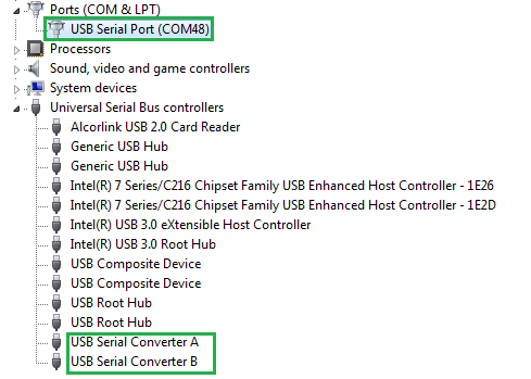
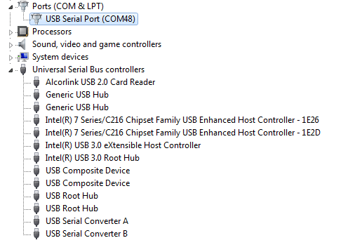
Open device manager and check the following drivers are installed. One USB Serial Port Driver and TWO USB Serial Converter Driver as Shown below. Then you can skip driver installation procedure and start working with Configuring FPGA using Vivado.
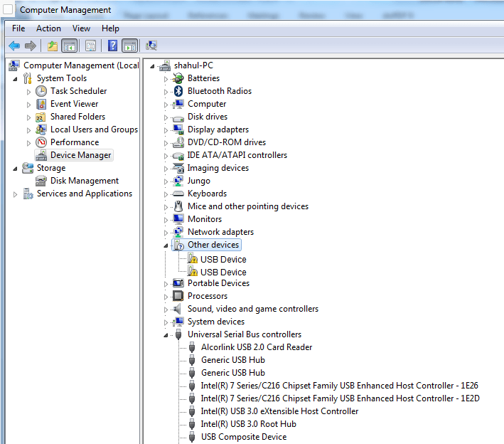
If the drivers are not installed you could see the USB device under Other Devices Category as shown below. Then you have to follow the driver installation steps given below.
Step1: Download and install virtual com port USB Driver for FTDI Chip.
http://www.ftdichip.com/Drivers/VCP.htm
Step2: Install driver by right click downloaded file and run as administrator
Step3: Connect Micro USB cable to FPGA kit U9 Port and another end to PC USB Port.
Step4: Open Device Manager. There are 2 other devices detected without drivers as shown in figure.
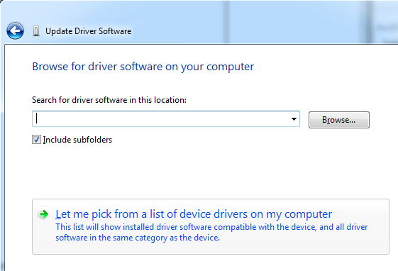
Step5: Right Click on the first USB device and select update driver.
Now select let me pick from the list of device drivers from my computer as shown below.
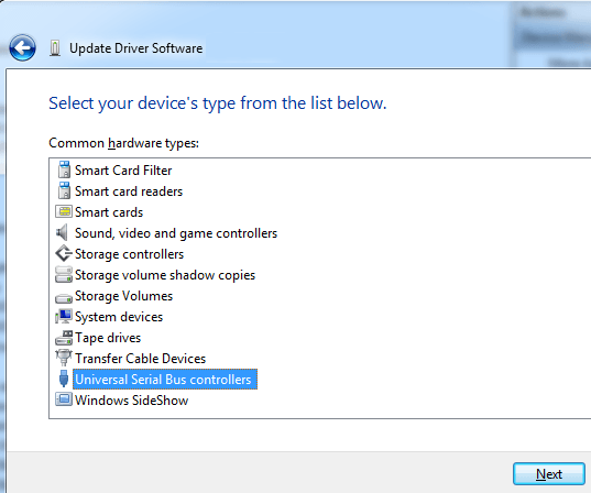
Step6: Now Select USB Serial Bus Controllers and click next.
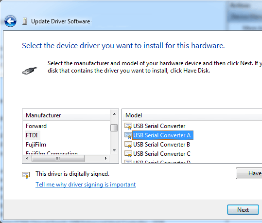
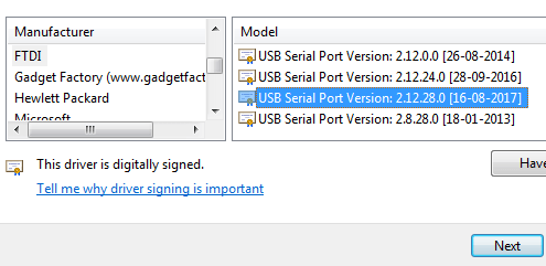
Step7: Select FTDI under manufacturer and select USB Serial converter A under model. (If multiple driver with Serial converter A present select latest version)
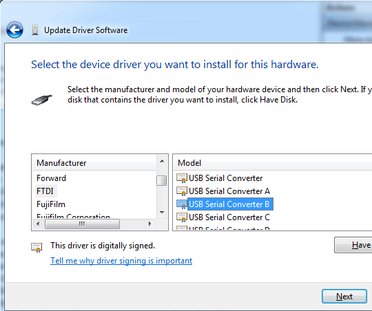
Step8: Repeat step 5 to step 7 for second unknown device. On step 7 select USB Serial Converter B instead A.
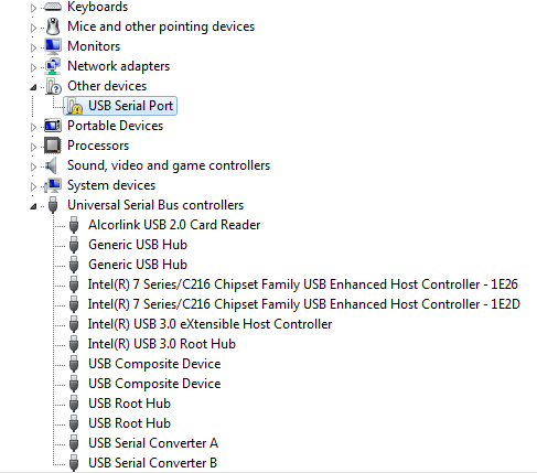
Step9: Now both USB Serial Convertor A and USB Serial Convertor B are detected under USB Controllers. But there another driver needs to be installed for USB Serial Port.
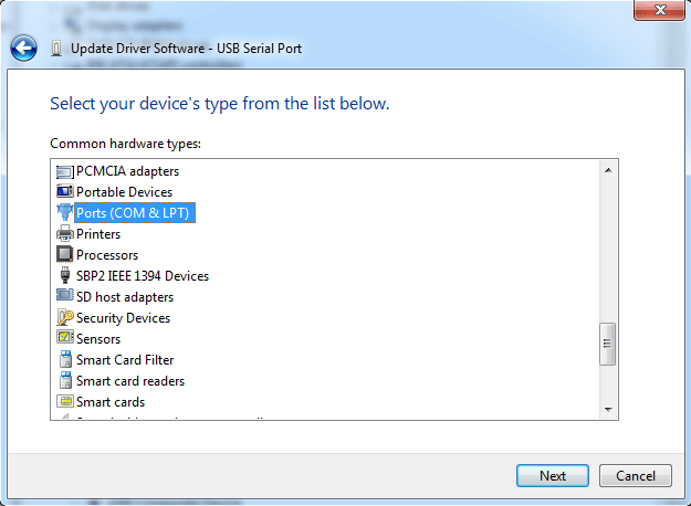
Step10: To install USB Serial Port, Right click and select update drive. Now select let me pick from the list of device drivers from my computer as shown below.
Step11: Select Ports (COM & LPT) option and click next.
Step12: Select FTDI under manufacturer and Select USB Serial Port under Model.
Step13: Now Drivers are installed and devices are detected under Ports and USB Controllers section.
Programming EDGE Board Artix 7 FPGA using Vivado Design Suite
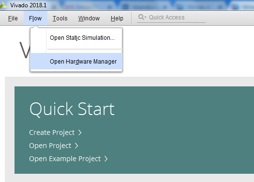
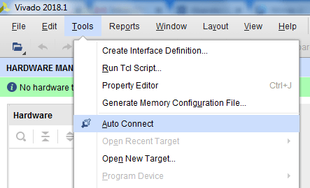
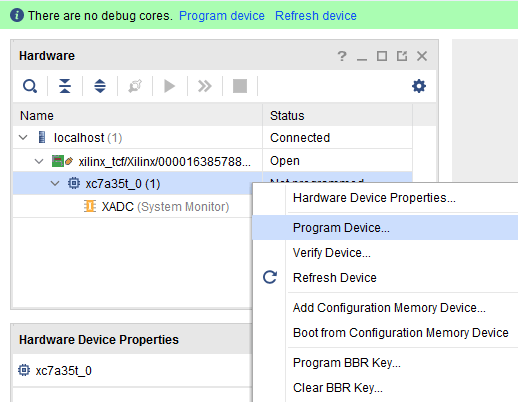
• Connect EDGE Artix 7 FPGA Kit to PC through USB cable and Turn On the kit.• Open “Hardware Manager -> Open Target -> Auto Connect
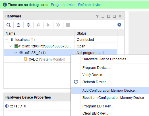
• If the device is detected successfully, then select “Program Device” by right click on the target device “xc7a35t_0” as shown below
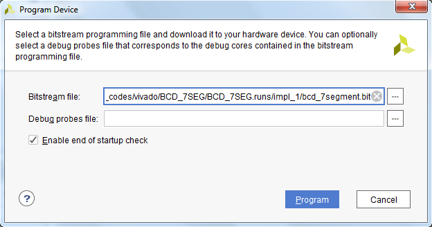
• Browse the Bit file need to be downloaded to the Artix 7 FPGA and click Program.
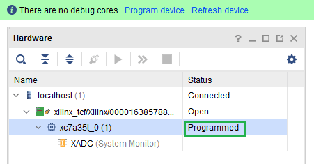
• Once the Program Succeeds, Done LED D1 light up on EDGE Artix 7 FPGA kit.
Programming Quad SPI FLASH Memory using Vivado Design Suite
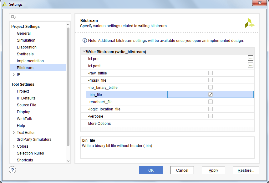
• Open “Bitstream Settings”, check “-bin_file*” checkbox and click OK.
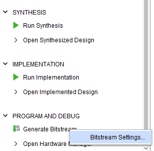
• Click on “Generate Bitstream” to generate your bit and bin file.
• Connect EDGE Artix 7 FPGA Kit to PC through USB cable and Turn On the kit.
• Open “Hardware Manager -> Open Target -> Auto Connect
• If the device is detected successfully, then select “Add Configuration Memory Device” by right click on the target device “xc7a35t_0” as shown below.
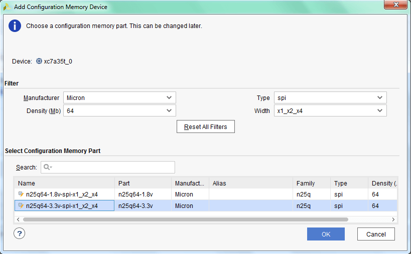
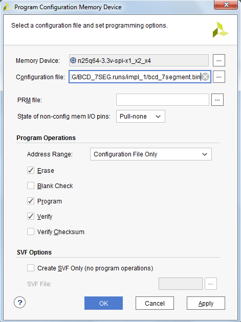
- Select the SPI FLASH memory. It can be micron memory device “n25q64-3.3v-spi-x1_x2_x4” or Spansion memory device “s25fl064l-spi-x1_x2_x4” then click OK.
Note: Check the name marking on U14 IC in the board to identify the flash memory used
• Now Dialog box open and ask for configuration Memory. Click Ok.
• Browse the bin file to be programmed in the SPI FLASH Memory and click Program.
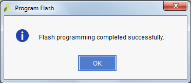
• Once the Program succeeds the following Dialog Box display the success message.
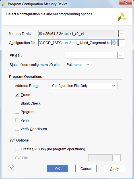
• To erase the PROM file, untick Program and verify option from Program Configuration Memory Window and click OK as shown in figure.
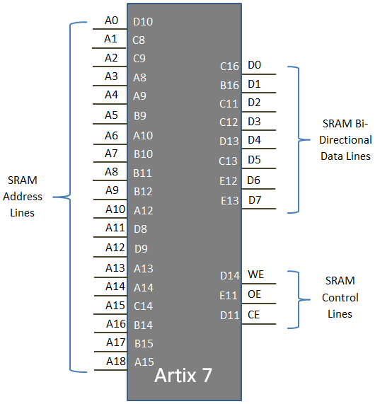
Appendix A – SRAM (Replaced with SDRAM on new boards)
The EDGE Board includes 512 KB of Static Random-Access Memory (SRAM). This memory has a standard, easy to use parallel interface with 19 address signals, 8 bi-directional data signals, and 3 control signals. The part used is the ISSI IS61WV5128BLL-10. The interface is fully documented in ISSI’s datasheet for the part.
The onboard SRAM is very useful for microblaze designs that would like to provide the processor with additional memory. To do this, the SRAM can be controlled with Xilinx External Memory Controller IP core.
-
 EDGE Artix 7 FPGA Development Board₹ 13,750