Table of Contents
Introduction
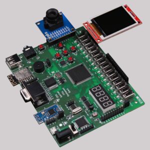
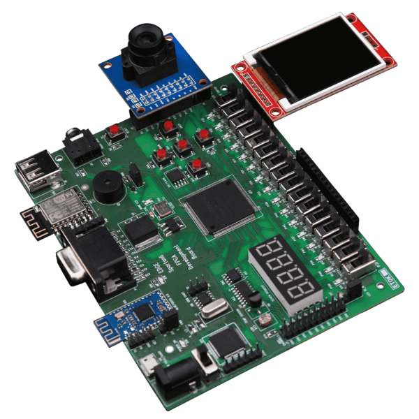
EDGE Spartan6 FPGA Development board is the feature rich development board with Spartan6 FPGA, SPI FLASH, Wi-Fi, Bluetooth, ADC, DAC, LCD, 7 segment Display, VGA, PS2, Stereo Jack, buzzer, Push Button, Slide Switch, LED, Temperature Sensor and LDR. The Board also provides additional interface like CMOS Camera and TFT Display at the expansion connectors.
The EDGE board provides USB JTAG interface for Programming and Debugging. It also provides USB UART interface.
Board Applications
• Wireless control
• Environment monitor
• IoT (Internet of Things)
• Product Prototyping
• Image Processing
• Video Processing
• Audio Processing
Board Features
• Xilinx XC6SLX9 TQG144C Spartan-6 FPGA IC
• 8MB SPI FLASH Memory
• On-Board USB JTAG Programmer
• USB to UART Interface
• WIFI Interface
• Low Power Bluetooth Interface
• 12 bit VGA Interface
• 8 Channel SPI ADC
• Temperature Sensor
• LDR Interface
• SPI DAC
• 2×16 LCD Display
• 4 Digit Seven Segment Display
• 5v Buzzer
• PS2 compatible USB interface
• CMOS Camera Interface
• TFT Display Interface
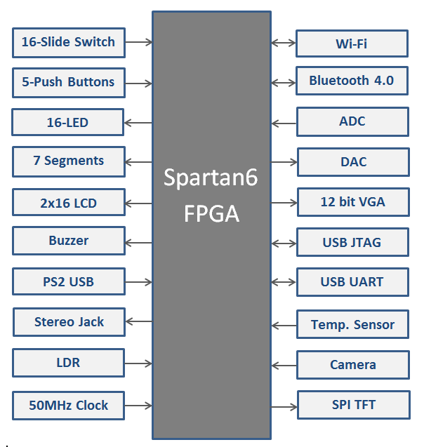
Block Diagram of EDGE Spartan 6 FPGA Development Board
Power Supply
EDGE Spartan6 development board can get 5V power from either USB JTAG Port U6 or External Power Supply connector J1. Switch SW3 can be used to select the source of power from USB or External Power Supply.
Board consist of 2 Voltage regulators 3.3v and 1.2v. The Kit requires 3.3v supply for FPGA I/O and Auxiliary supply, Clock, USB Port, ADC, DAC, FLASH, and so on. The 1.2v power supply is dedicated for FPGA Core voltage.
Caution: Only 5v Supply must be provided to the board either from external source or USB connector.
Programming hardware
FPGA can be configured either from USB JTAG using Xilinx software or by on-board SPI FLASH Memory.
FPGA configured through JTAG gets erased when the power supply is removed or by pressing reset button SW1.
To store the data permanently on FPGA, we have to store the configuration bit file to SPI FLASH Memory. It automatically reconfigures the FPGA after reset or Power on.
The EDGE Spartan6 FPGA Development board is fully compatible with Xilinx ISE, EDK, System Generator and Chipscope Pro Tools at ease with on-board USB JTAG Interface.
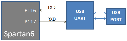
USB UART
The EDGE Board includes FT2232 IC acts as USB UART Bridge to communicate board with windows PC COM port interface.
The UART Transmitter and Receiver lines of FTDI chip is directly connected to the Spartan6 FPGA I/O pins for USB UART Communication.
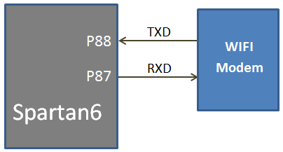
WIFI Communication
The EDGE Board contains On-board ESP8266 12F WIFI Module connected with Spartan6 FPGA through serial interface. The ESP WIFI Modem helps to communicate FPGA with cloud. The Data can be stored and retrieved from the cloud with the help of AT Commands. The range of communication for WIFI modem is 50 – 100 meter distance.
Note: To enable power supply to the WIFI Modem, place jumper at Enable and centre pin of J11. To disable power, place jumper at Disable and centre pin of J11.
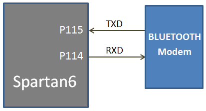
Bluetooth Communication
The EDGE contains low power Bluetooth 4.0 BLE interface on-board. The Bluetooth is serially interfaced with FPGA with Transmit and Receive lines.
Note: To enable power supply to the Bluetooth Modem, place jumper at Enable and centre pin of J13. To disable power, place jumper at Disable and centre pin of J13.
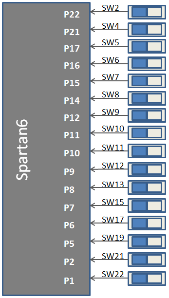
Slide Switches
The EDGE board includes 16 SPDT slide switches for digital input. These digital inputs are connected to Spartan6 FPGA through resistors for protection against short circuit. Slide switch outputs constant high or constant low based on the user changing its position.
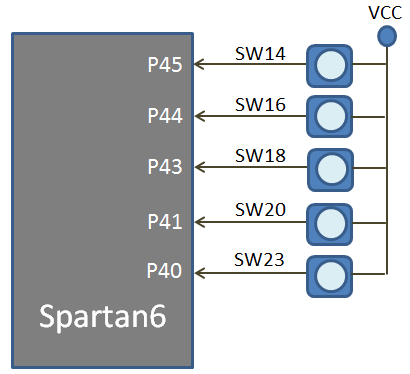
Push Buttons
The Board contains 5 Push buttons for providing momentary digital inputs. They are connected to FPGA lines through resistors to prevent short circuit. By default the switch is in Active low. When the user pressed the push button they are driven high.
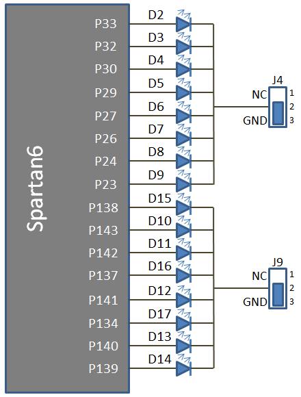
LEDs
The Kit consists of 16 LEDs for displaying digital outputs. These LED’s are connected with FPGA through a series resistor. Logic High signal turns ON LED and Logic Low signal turns OFF LED to demonstrate the digital output.
Note: To enable LEDs, Jumper needs to be placed at ground position at J4 and J9.
The J4 connector enables LEDs D2 to D9.
The J9 connector enables LEDs D10 to D17.
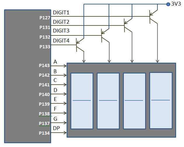
Seven segment Display
The EDGE Board consist of 4 digit 7 segment displays with common anode. Each of the seven segment contains LEDs can be turned on by sending active low signal.
For example, to display digit 8 in the seven segments display. All the segments are enabled using active low ‘0’ signal.
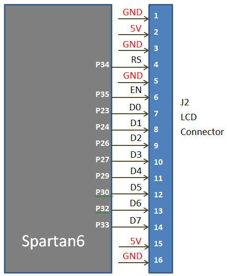
2×16 LCD
The EDGE board consist of 2×16 LCD interface at the female connector J2. LCD displays is interfaced in the 8 bit data mode, RS pin are used to select data/command mode and En are used to enable the LCD.
Note: R/W pin is connected to ground to keep LCD in always write mode.
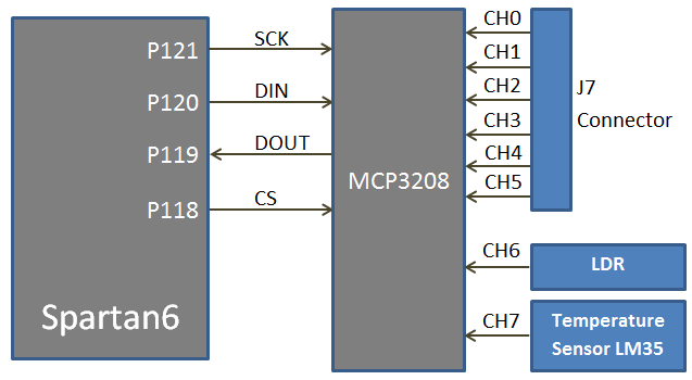
SPI ADC
The EDGE board contains Microchip MCP3208 8-channel 12-bit SPI ADC. ADC is connected to FPGA through 4 SPI lines. The SPI signals are Serial Clock, Data in, Data out, chip select.
Input Analog signal to ADC channel Ch0 – Ch5 are provided at male connector J7.
Light Detect Resistor LDR is connected at the ADC channel Ch6. LDR provides variable resistance based on the light intensity that falls upon it.
Temperature Sensor LM35 is connected at the ADC channel Ch7.
Refer MCP3208 Datasheet to learn more about its working.
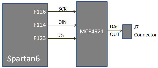
SPI DAC
The EDGE Board consist of Microchip MCP4921 SPI DAC to perform digital to analog conversion. The output is available at the male connector J7.
SPI interface provides Serial clock, Data input and chip select to FPGA with DAC. Spartan6 FPGA act as master and MCP4921 act as slave device.
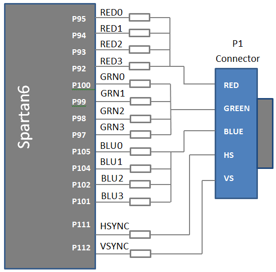
VGA
The EDGE Board contains 12 bit VGA interface to generate VGA signals from FPGA and display the output in the VGA monitor. The 12 bit VGA output the depth of 4096 colours in the Monitor. Series resistors are used to construct DAC to implement VGA interface.
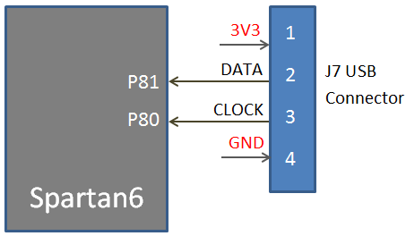
PS2
The EDGE board contains PS2 interface connected with FPGA through clock and data lines. PS2 interface is directly provided in the USB connector. Only USB keyboard reverse compatible with ps2 connector work on this port.
Note: 3.3v supply is provided to the PS2 interface to prevent over voltage on FPGA I/O lines.
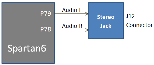
Stereo Jack
Stereo Audio Jack with low pass filter is connected on the FPGA I/O lines on the EDGE Board. Stereo Jack provides delta sigma audio output.
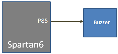
Buzzer
The Edge board contains piezo buzzer interface with FPGA through transistor. 5v Buzzer is used provide alert tone. Buzzer’s resonant frequency is 3.8 kHz (where you can expect its best performance).
Note: To enable Buzzer, place jumper at Enable and centre pin of J6. To disable power, place jumper at Disable and centre pin of J6.
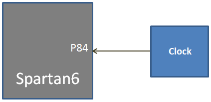
Clock
The Edge board contains 50 MHz Oscillator to provide clock input to the FPGA. The input clock can drive any or all of the four clock management tiles in the Spartan-6. Each tile includes two Digital Clock Managers (DCMs) and four Phase-Locked Loops (PLLs).
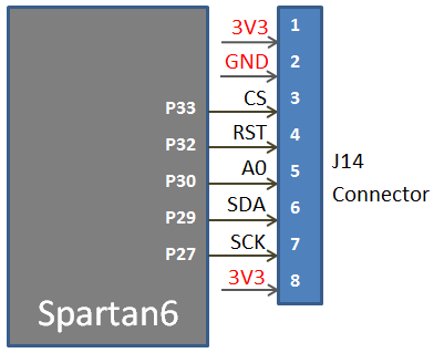
TFT Display
The EDGE Board contains TFT display interface at the J14 connector. TFT display communicates with FPGA through SPI protocol. SPI TFT is made of ST7732S SPI controller with 160×128 Display .
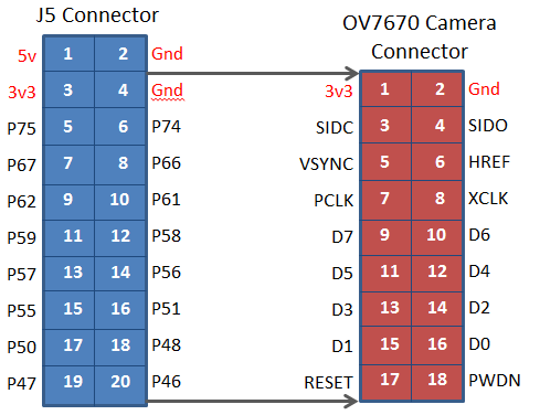
20 Pin Expansion Connector / CMOS Camera Interface
Expansion connector J5 provides 16 I/O lines from spartan6 FPGA to the external interface.
Note: To interface OV7670 CMOS Camera with EDGE Board. Leave pin1 and pin2 unconnected. Connect pin3 of expansion connector to pin1 of CMOS Camera.
Driver Installation
Step1: Download and install virtual com port USB Driver for FTDI Chip.
http://www.ftdichip.com/Drivers/VCP.htm
Step2: Install driver by right click downloaded file and run as administrator
Step3: Connect Micro USB cable to FPGA kit U2 Port and another end to PC USB Port.
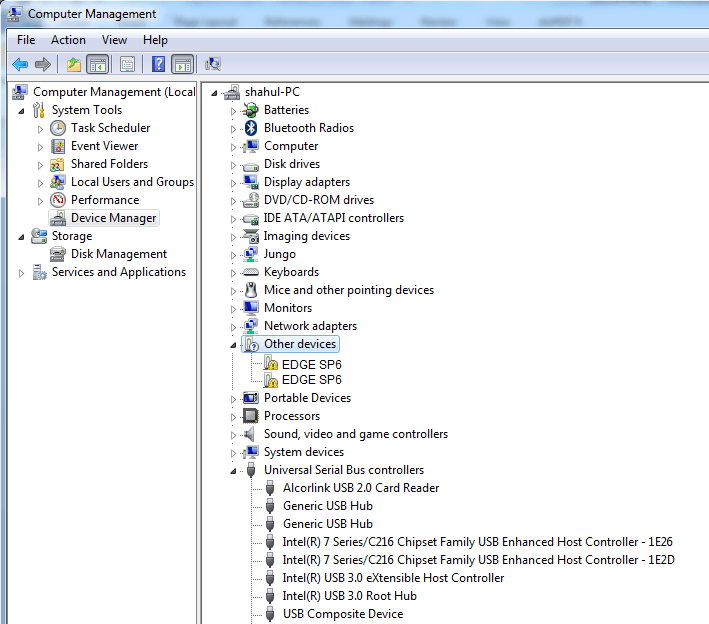
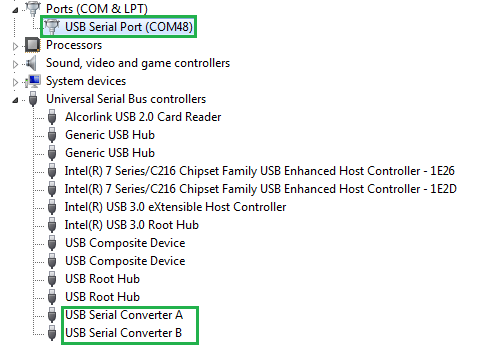
Step4: Open Device Manager. There are 2 other devices detected without drivers as shown in figure.
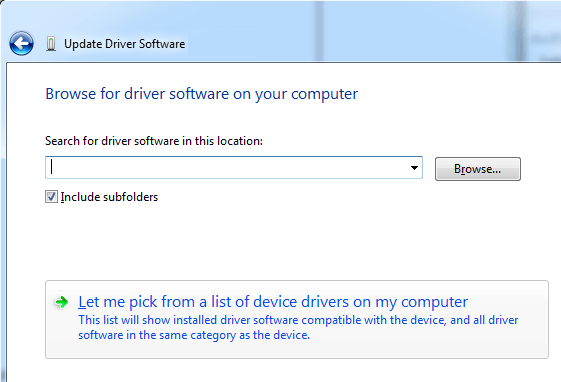
Step5: Right Click on the first unknown device and select update driver.
Now select let me pick from the list of device drivers from my computer as shown below.
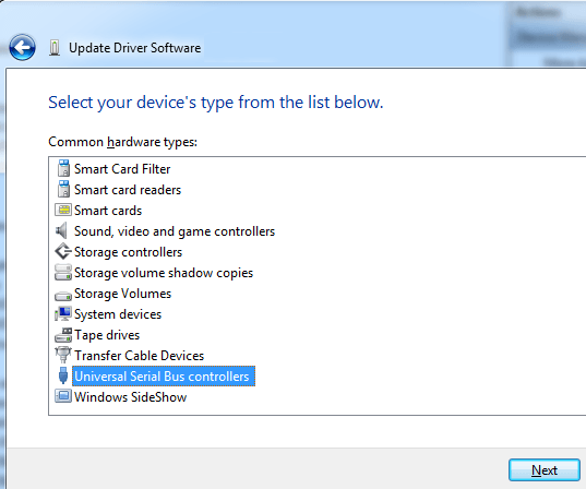
Step6: Now Select USB Serial Bus Controllers and click next.
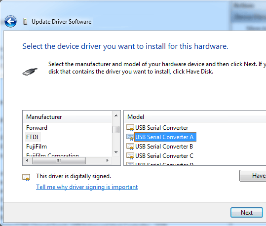
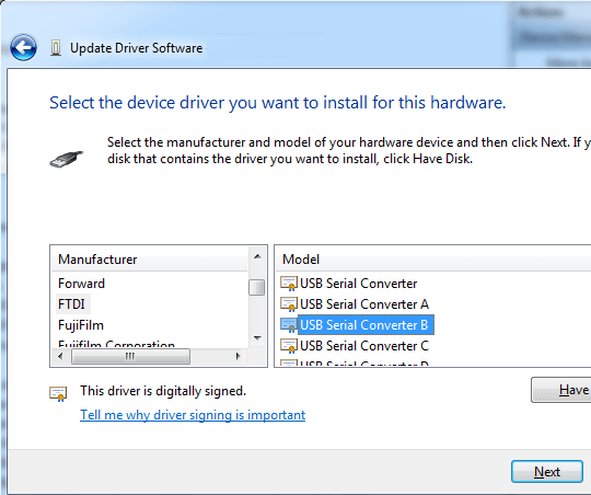
Step7: Select FTDI under manufacturer and select USB Serial converter A under model. (If multiple driver with Serial converter A present select latest version)
Step8: Repeat step 5 to step 7 for second unknown device. On step 7 select USB Serial Converter B instead A.
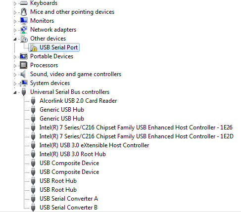
Step9: Now both USB Serial Convertor A and USB Serial Convertor B are detected under USB Controllers. But there another driver needs to be installed for USB Serial Port.
Step10: To install USB Serial Port, Right click and select update drive. Now select Browse computer for driver software and select let me pick from the list of device drivers from my computer as shown below.
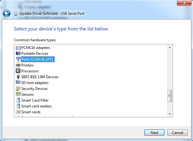
Step11: Select Ports option and click next.
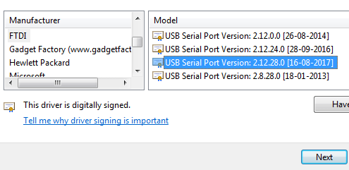
Step12: Select FTDI under manufacturer and Select USB Serial Port under Model.
Step13: Now Drivers are installed and devices are detected under Ports and USB Controllers section.
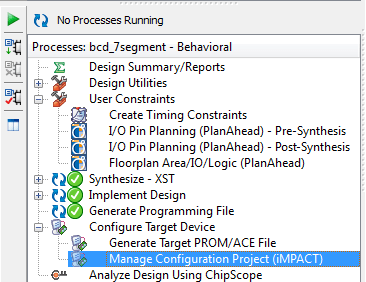
Programming EDGE Board Spartan 6 FPGA using Xilinx iMPACT
After Generating Programming File Select Manage Configuration Project to open iMPACT
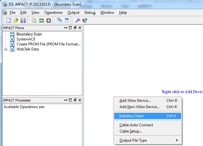
Now double click on Boundary scan option opens blank window on the right side.
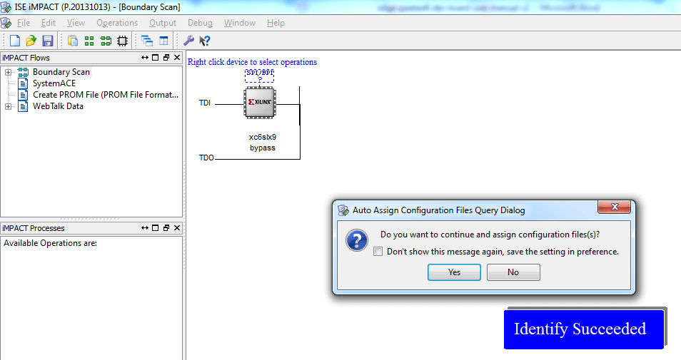
Right click on the blank window and select Initialize Chain.
Now XC6SLX9 FPGA detected and asking to assign configuration file to it. Click yes.
Now select filename.bit file
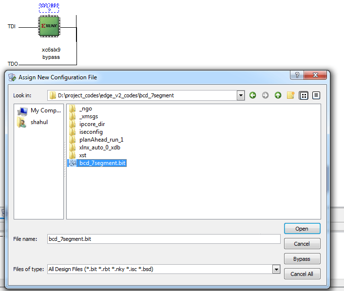
Now it ask for PROM device. Skip it by selecting No.
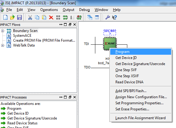
Now right click on Spartan6 FPGA and click program.
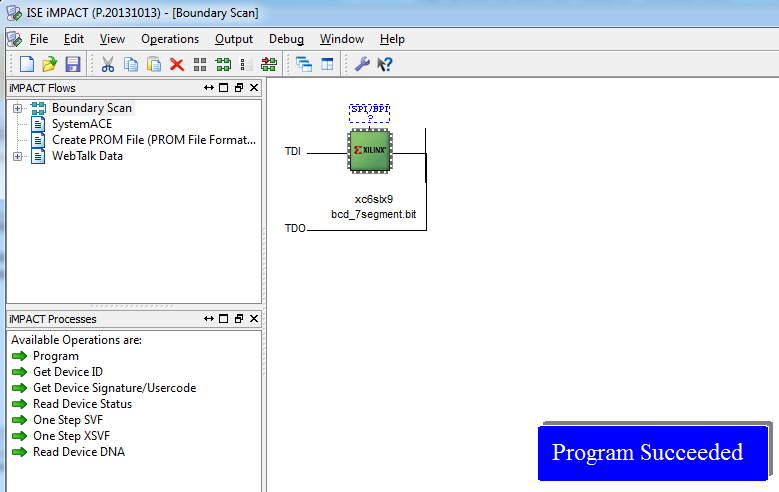
It displays Program Succeeded message and Done LED glow on EDGE Board for the indication of Programming completed.
Programming SPI FLASH Memory using Xilinx iMPACT
To Program SPI Flash, Set the following operating system environment variable
XIL_IMPACT_SKIPIDCODECHECK=1
The procedure for setting an environment variable varies by operating system. The following sequence shows how to add an environment variable within the Microsoft Windows 7 Professional operating system:
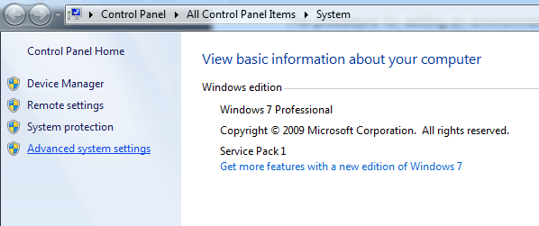
a) Click the Windows Start Button and open the “Control Panel.”
b) Within the “Control Panel” click “System and Security” followed by “System,” which will open the “Basic Information” window.
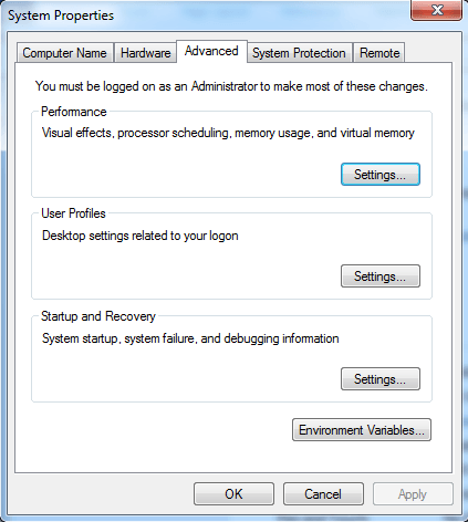
c) Click “Advanced system settings” to open the “System Properties” window
d) In the “System Properties” window, select the “Advanced” tab and then click the “Environment Variables” button which will open an “Environment Variables” window
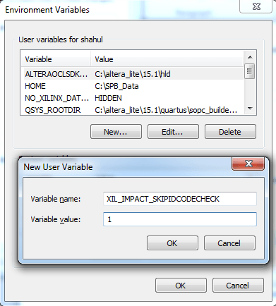
e) In the “Environment Variables” window click one of the two “New…” buttons to create either a User variable or a System variable. In Figure below, a new User variable is being created.
f) In the “New User Variable” window, enter “XIL_IMPACT_SKIPIDCODECHECK” for the Variable name and “1” for the Variable value. Click the “OK” button to add the environment variable.
After Setting environment variable open Xilinx iMPACT Tool.
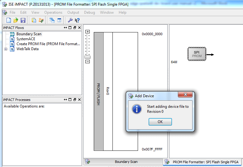
Select Create PROM file in the iMPACT window
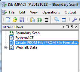
PROM File Formatter dialog box opens.
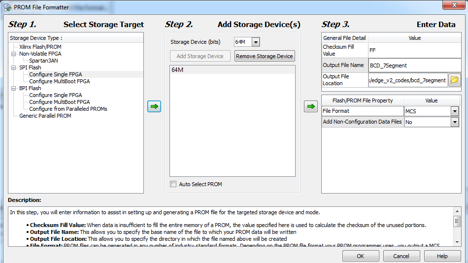
Now select configure single FPGA under SPI FLASH in step1.
Then Select Storage Device to 64M and click Add Storage Device in step2.
Then Select output file location and specify output file name in step 3
After completing 3 steps click ok.
Now the following window opens and click ok in the add device dialog box.
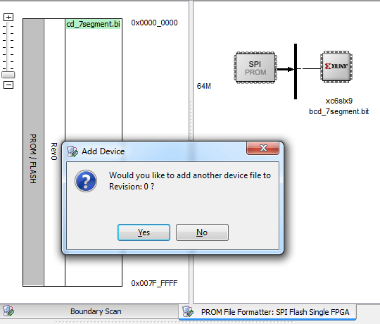
Now select bit. It will ask for adding new device. Click NO
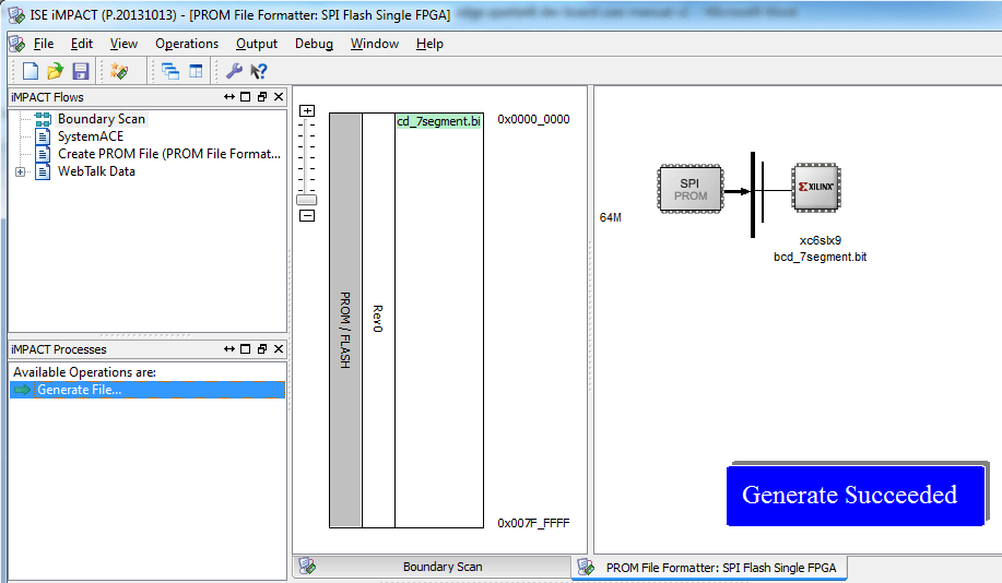
Now Click generate file option under iMPACT Process to generate MCS file.
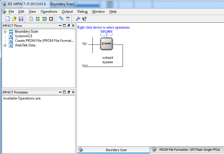
Now double click boundary scan option and do initialize chain to detect Spartan 6 FPGA.
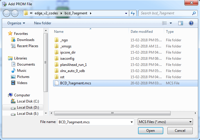
Now click double click SPI/BPI option at the top FPGA IC to select MCS file for SPI FLASH Memory.
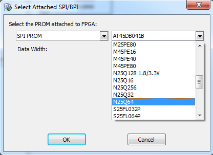
Now Select N25Q64 in the SPI PROM Dialog box.
Now FLASH Added at the top of FPGA. Right click PROM and select Program option.
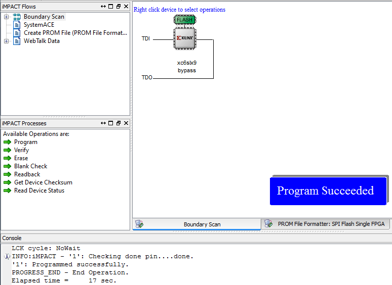
Now Program Succeeded and done LED is glowing on the EDGE Board.
To erase the PROM file, right click FLASH symbol at the top and select Erase option to successfully erase the SPI FLASH Data.