This tutorial explains the step by step procedure to create a Vivado project, create source files, synthesize the design, Implement the design and finally verify the functionality in FPGA using the EDGE 7 Series FPGA board.
Step 1: Open Vivado design Suite by selecting
Start > All Programs > Xilinx Design Tools > Vivado 2019.1 > Vivado 2019.1
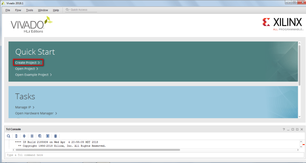
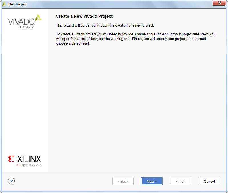
Step 2: Click Create New Project and click next to open new project wizard.
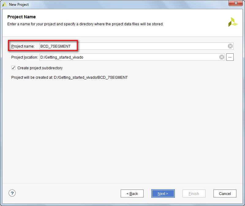
Step 3: Select Project directory and mention new project name.
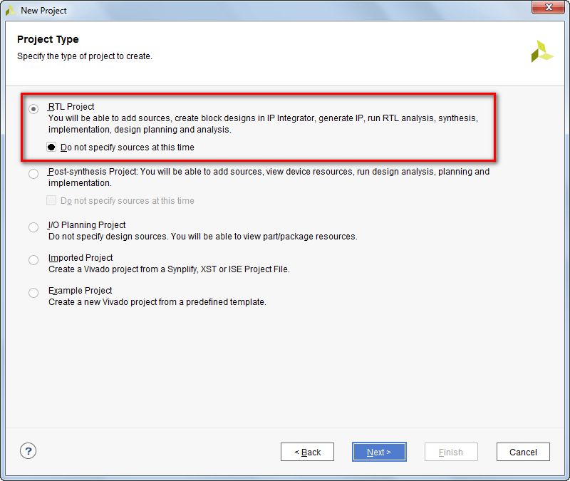
Step 4: Select RTL Project and check Do not specify sources at this time.
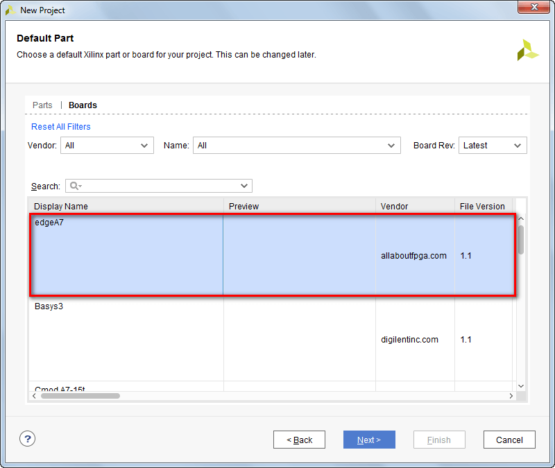
Step 5: Click Boards and
select edgeS7 in Part Selection window or select Part XC7S15FTGB196-1 from the list of parts available for EDGE Spartan 7 Board
or
select edgeA7 in Part Selection window or select Part XC7A35TFTG256-1 from the list of parts available for EDGE Artix 7 Board
or
select edgeZ7_10 in Part Selection window or select Part XC7Z010CLG400-1 from the list of parts available for EDGE ZYNQ Z10 Board
or
select edgeZ7_20 in Part Selection window or select Part XC7Z020CLG400-1 from the list of parts available for EDGE ZYNQ Z20 Board.
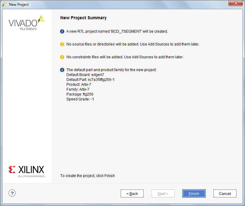
Step 6: Now the New Project summary display with project details selected.
Step 7: Now the Vivado tool opens with Flow Navigator on left and Project Manager on right. Flow Navigator display the list of process involved from HDL input creation to bit file output generation. Project manager consist of Source, Workspace and Report Window.
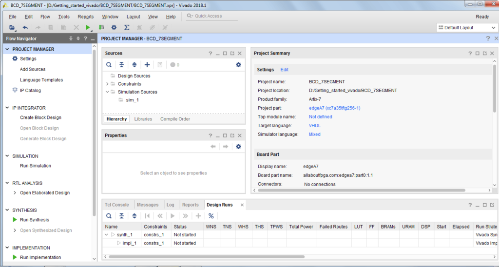
Source Window displays Design Sources (VHDL, Verilog), Constraints (XDC) and Simulation sources. Workspace Window is used to create and view HDL/XDC files. Report Window consist of TCL console, Messages, Logs, Reports and Design Rules
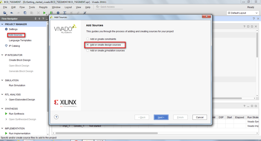
Step 8: Now click Add source and select Add create design sources
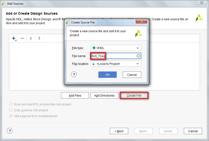
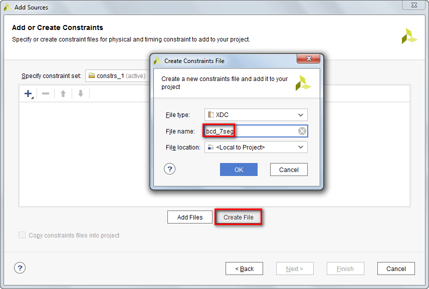
Step 9: Click create file and select file type and file name as bcd_7seg
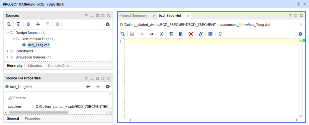
Step 10: Double click on the bcd_7seg.vhd at source window to open on the right side.
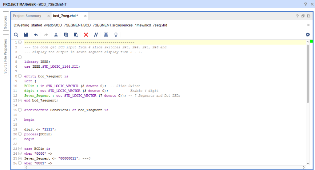
Step 11: Copy the following BCD to 7 seven segment VHDL code and paste on the text editor opened.
-------------------------------------------------------
--- the code get BCD input from 4 slide switches SW2, SW4, SW5, SW6 and
--- display the output in seven segment display from 0 - 9.
------------------------------------------------------------
library IEEE;
use IEEE.STD_LOGIC_1164.ALL;

entity bcd_7segment is
Port (
BCDin : in STD_LOGIC_VECTOR (3 downto 0);  -- Slide Switch
digit : out STD_LOGIC_VECTOR (3 downto 0);        -- Enable 4 digit
Seven_Segment : out STD_LOGIC_VECTOR (7 downto 0)); -- 7 Segments and Dot LEDs
end bcd_7segment;

architecture Behavioral of bcd_7segment is
begin
digit <= "1111";
process(BCDin)
begin
case BCDin is
when "0000" =>
Seven_Segment <= "00000011"; ---0
when "0001" =>
Seven_Segment <= "10011111"; ---1
when "0010" =>
Seven_Segment <= "00100101"; ---2
when "0011" =>
Seven_Segment <= "00001101"; ---3
when "0100" =>
Seven_Segment <= "10011001"; ---4
when "0101" =>
Seven_Segment <= "01001001"; ---5
when "0110" =>
Seven_Segment <= "01000001"; ---6
when "0111" =>
Seven_Segment <= "00011111"; ---7
when "1000" =>
Seven_Segment <= "00000001"; ---8
when "1001" =>
Seven_Segment <= "00001001"; ---9
when others =>
Seven_Segment <= "11111111"; ---null
end case;
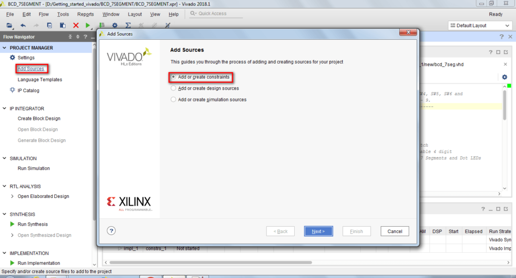
Step 12: Now again select the Add Source and select Add or create constraints
Step 13: Click create file and mention file type and file name
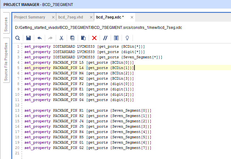
Step 14: Copy the following XDC File and paste it on the XDC editor window created.
Refer EDGE Spartan 7 XDC File for Spartan 7 board.
Refer EDGE Artix 7 XDC File for Artix 7 board.
Refer EDGE ZYNQ SoC XDC File for ZYNQ SoC board.
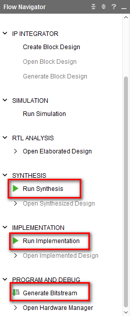
Step 15: Save bcd_7seg.vhd and bcd_7seg.xdc file created and perform synthesis, Implementation and generate bitstream by click them one by one in Flow Navigator
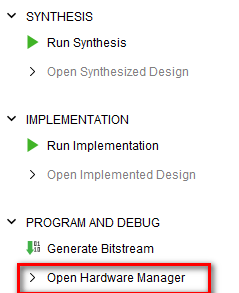
Step 16: Click Open Hardware Manager in Flow Navigator to program the bit file.
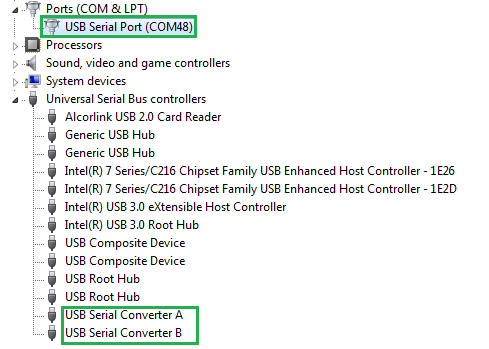
Step 17: Connect EDGE Artix 7 FPGA Kit to PC through USB cable and Turn On the kit. Open device manager to verify drivers are installed as shown below. Otherwise install USB Programmer drivers by referring kit user manual driver installation section.
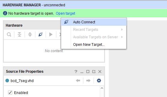
Step 18: To detect FPGA, Do Hardware Manager -> Open Target -> Auto Connect
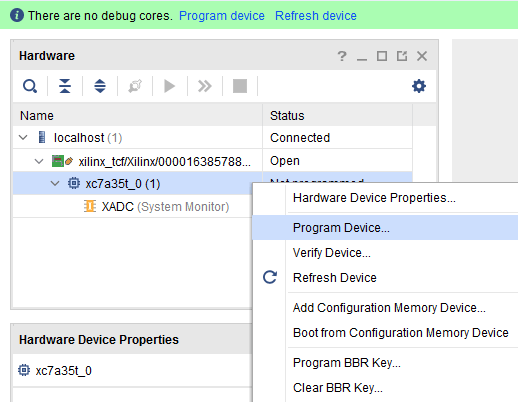
Step 19: If the device is detected successfully, then select Program Device by right click on the target device xc7a35t_0 as shown below
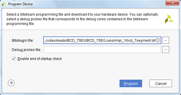
Step 20: Browse the Bit file need to be downloaded to the Artix 7 FPGA and click Program.
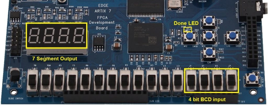
Step 21: Once the Program Succeeds, Done LED D1 light up on EDGE Artix 7 FPGA kit. The BCD to 7 Segment Converter get BCD input from 4 slide switches SW3, SW4, SW5, SW6 and display the corresponding output in seven segment display from 0 – 9.
-
 EDGE Artix 7 FPGA Development Board₹ 13,750