

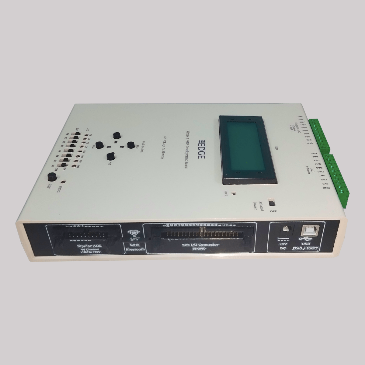
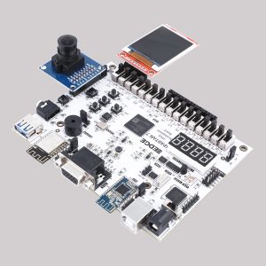
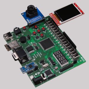
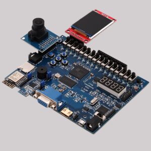
EDGE Kintex 7 FPGA Development Board
Product Includes
- EDGE Kintex 7 FPGA Development Board
- USB Cable
- 12v DC Adaptor
Description

Additional information
| FPGA | Kintex 7 XC7K160T FPGA |
|---|---|
| DDR3 | 1 GB DDR3 32 bit Memory |
| USB Communication | USB 3.0 High Speed Communication |
| USB JTAG | Onboard USB JTAG for programming |
| USB UART | Isolated USB UART |
| Power | Onboard Isolated Power |
| SPI FLASH | 128Mb FLASH Memory |
| wireless communication | WIFI/Bluetooth for wireless communication |
| Slide Switch | 8 SPDT Slide Switch for user input selection |
| LED | 8 LED for user output |
| Push Button | 4 Push Button for User Input |
| LCD | 20X4 LCD |
| Clock | 50 MHz Clock |
| Bipolar ADC | Bipolar SPI ADC |
| Unipolar ADC | Unipolar SPI ADC |
| DAC | SPI DAC |
| I/O Connector | 100 I/O |
Reviews
There are no reviews yet.