Table of Contents
Setting up and programming the EDGE ZYNQ Board for Processing System (PS)
In every chapter, the board will need to be setup and programmed. This section describes how to accomplish this.
Hardware Required:
– EDGE ZYNQ 7000 SoC FPGA Development board
– USB cable
Software Required:
– Vivado 2018.1
– SDK 2018.1
This tutorial explains the step by step procedure to demonstrate the EDGE ZYNQ Processing system(PS) demo for UART, Ethernet, Memory Test and Push Butoon LED by creating a Vivado SDK Project.
Vivado Project Creation
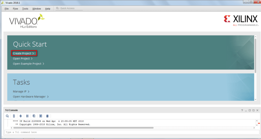
Open Vivado design Suite by selecting
Start > All Programs > Xilinx Design Tools > Vivado 2018.1 > Vivado 2018.1
Click Create New Project and click next to open new project wizard.
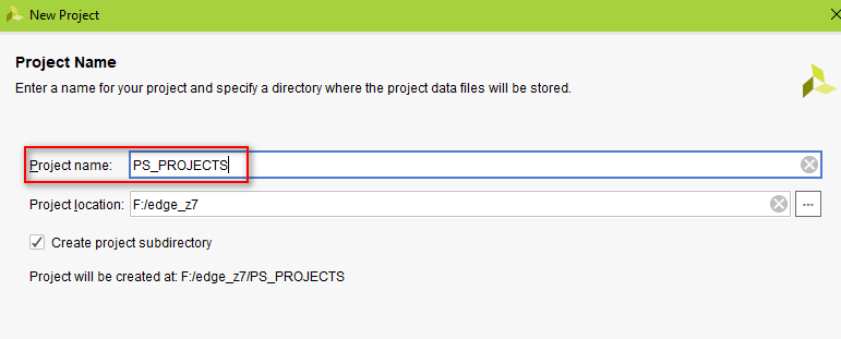
Select Project directory and mention new project name.
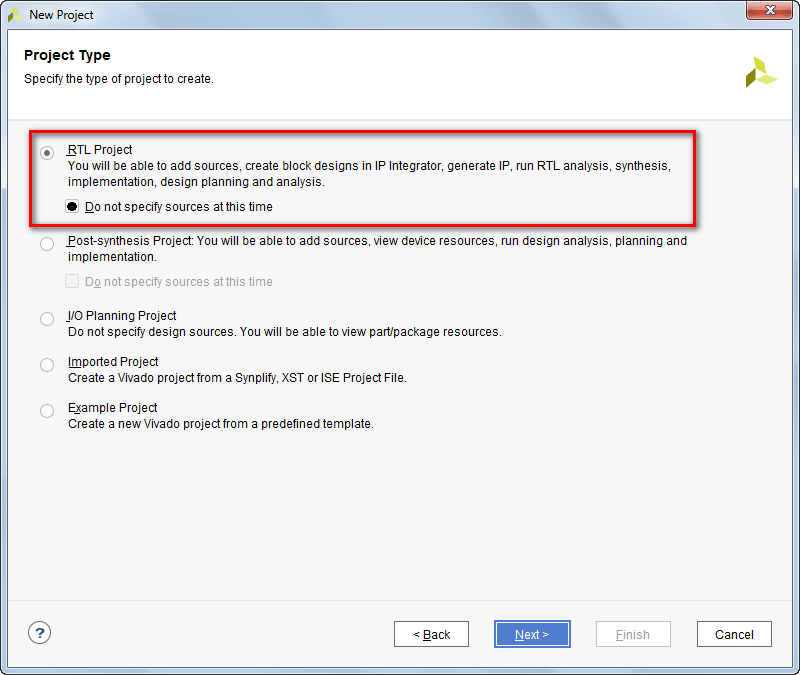
Select RTL Project and check Do not specify sources at this time.
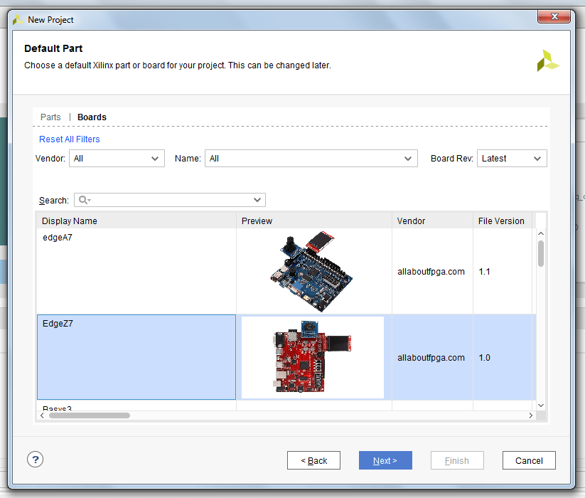
Click Boards and select EdgeZ7 in Part Selection window or select Part XC7Z010CLG400-1 from the list of parts available.
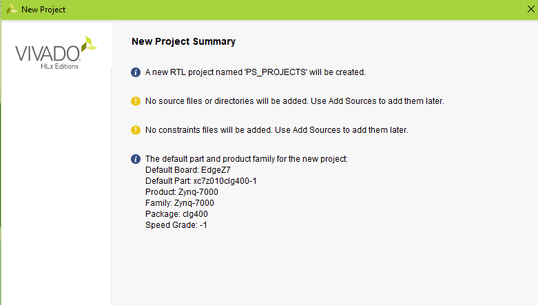
Now the New Project summary display with project details selected.
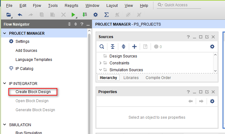
Now the Vivado tool opens with Flow Navigator on left and Project Manager on right. Flow Navigator display the list of process involved from HDL input creation to bit file output generation. Project manager consist of Source, Workspace and Report Window.
Source Window displays Design Sources (VHDL, Verilog), Constraints (XDC) and Simulation sources. Workspace Window is used to create and view HDL/XDC files. Report Window consist of TCL console, Messages, Logs, Reports and Design Rules
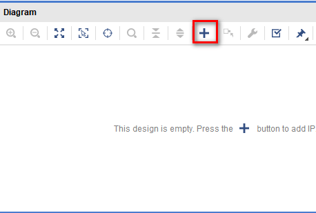
Click “Create Block Design”, designed to create a Block
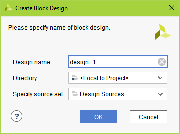
“Design name “do not make changes, keep the default” design_1 “, where you can modify it as needed, but the name to be as brief as possible, otherwise there will be problems in Windows compiler.
Click on “Add IP” shortcut icon
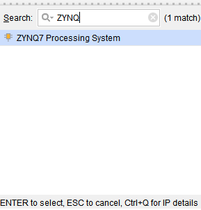
Search “zynq”, double-click in the search results list “ZYNQ7 Processing System”
Double-click Block figure “processing_system7_0”, the related parameters
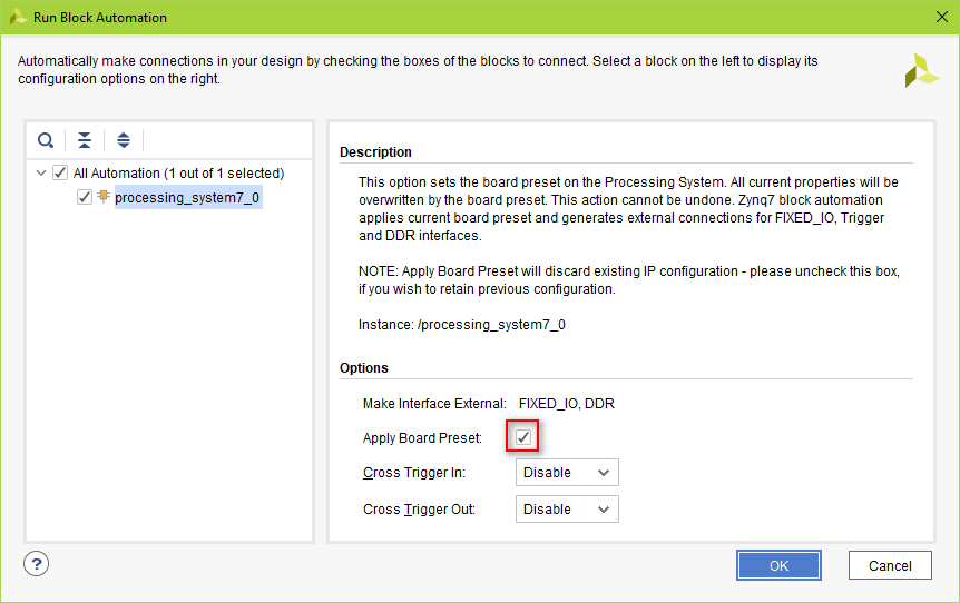
The connection automation tool will add the required logic blocks for the demo. Select Run Block Automation highlighted in blue.
Click the Run Block Automation link
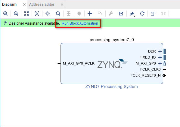
Connect FCLK_CLK0 to M_AXI_GP0_ACLK
Your Zynq block should now look like the picture below.
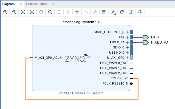
From the diagram, we can find the required PS pins are connected with the ZYNQ processor
The connected interfaces
Double-click Block figure “processing_system7_0”, the related parameters with processing system are
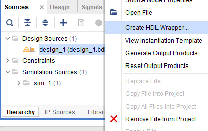
Select Block design, right “Create HDL Wrapper …”, create a Verilog or VHDL file
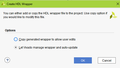
Keep the default option and click “OK”
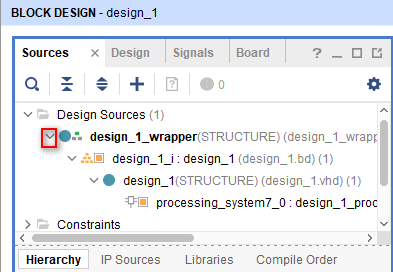
Unfolding can see PS is used as a normal IP.
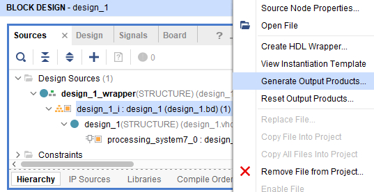
Select block design, right “Generate Output Products”
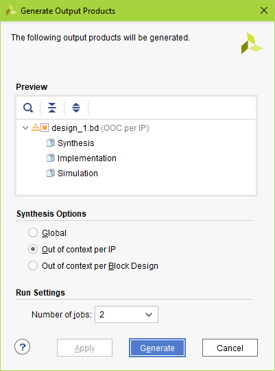
Click on “Generate”
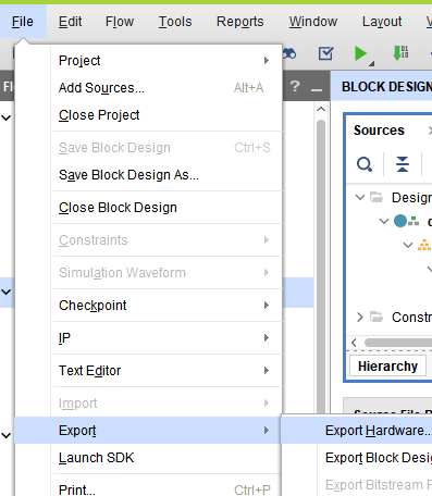
In the menu bar “File -> Export -> Export Hardware …” to export hardware information, here it contains a PS configuration information.
In the dialog box, click “OK “, because the experiments are only using the serial port PS, PL is not required to participate, there is no enable” Include bitstream “
SDK Debugging
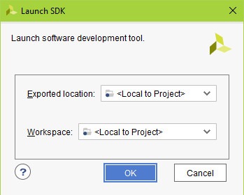
Click Vivado menu “File -> Launch SDK”, starting SDK

Click OK.
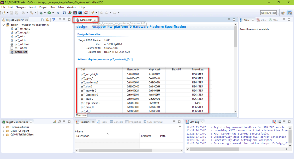
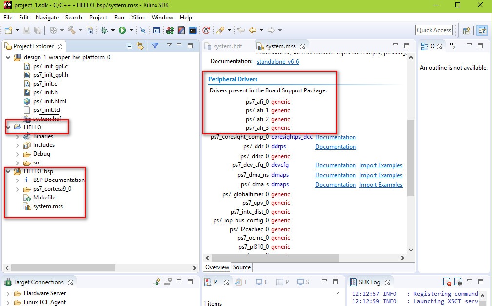
Start SDK we will see a folder, there is a “system.hdf” file named, this file contains the Vivado Information hardware design, software developers can use to, you can see a list of PS register end peripherals.
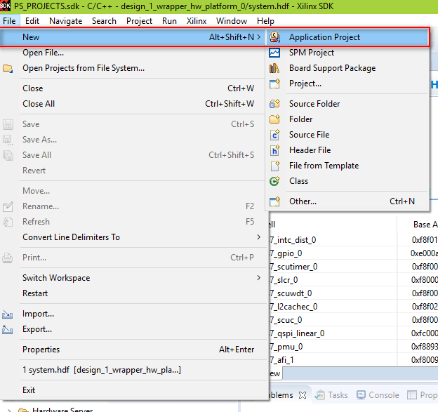
1. UART testing
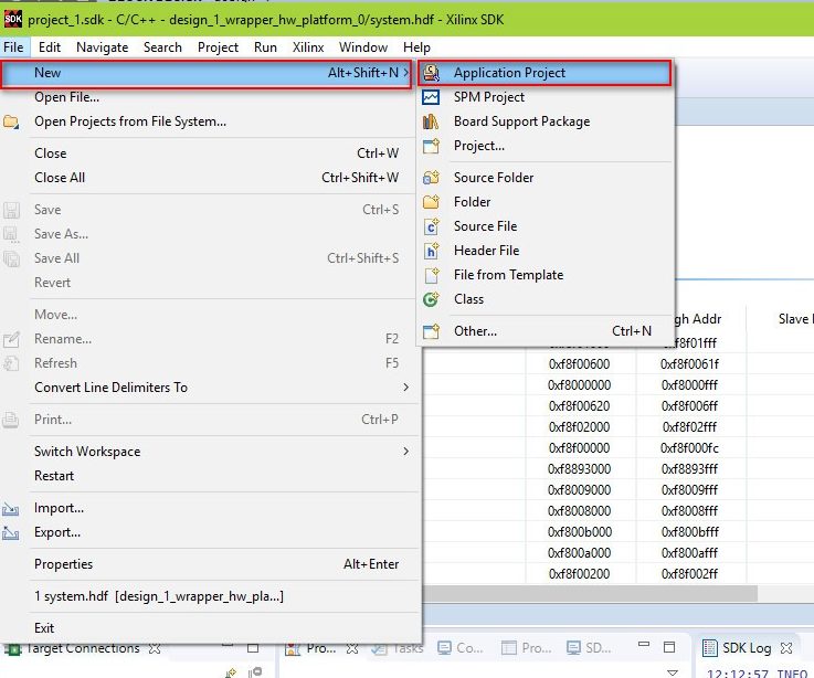
In SDK menu “New -> Application Project”, to create Hello World Application Project
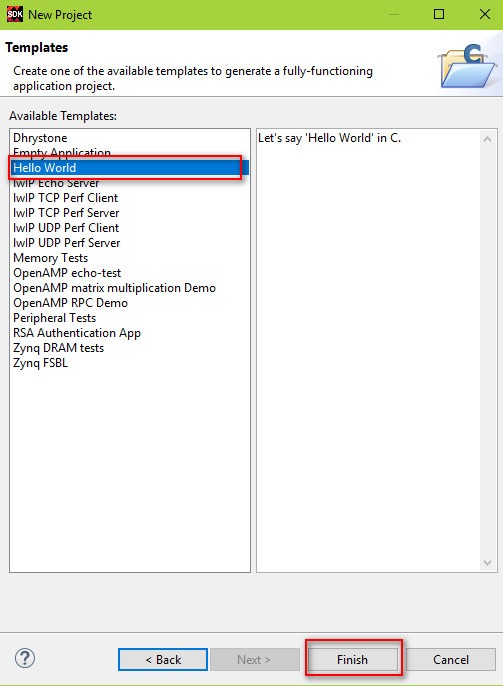
Enter Project name as “HELLO”
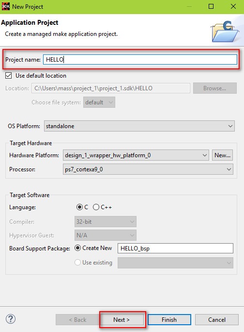
In the Template Selection window, select “Hello World”, click “Finish”
SDK create a “HELLO” directory, “HELLO_bsp” directory, you can find a lot of useful information in the “HELLO_bsp” directory, and where there are “BSP Documentation” contains a number of peripheral PS API descriptions.
Connect the EDGE ZYNQ FPGA development board to the PC
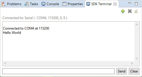
At the bottom of the SDK tool, you can see the SDK Terminal. Click on the + symbol.

Select Com Port detected from FPGA USB UART. Also select Baud Rate as 115200 and click OK

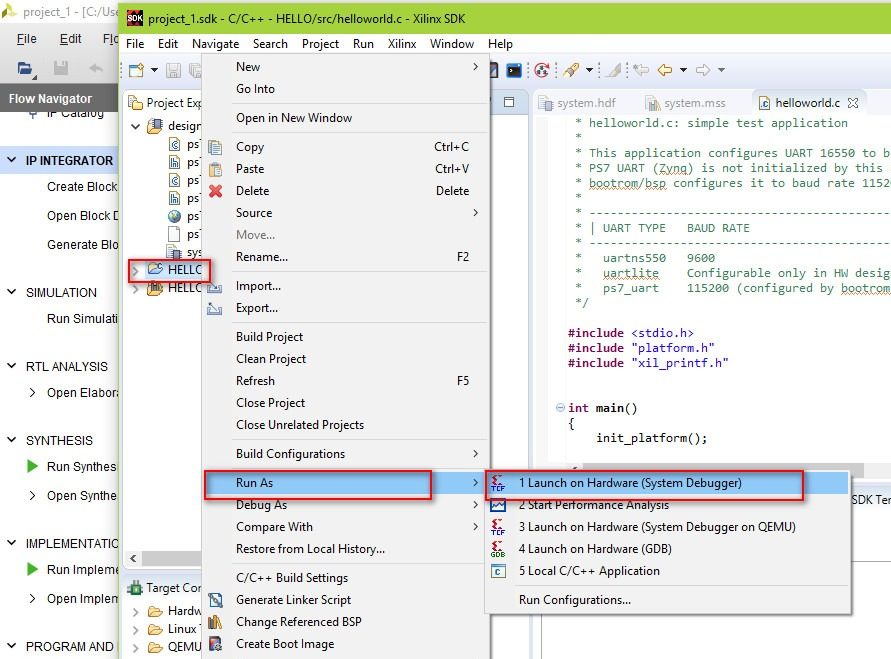
9. Right Click on the “HELLO“ project select Run AS Launch on Hardware
The output can be seen on the terminal window as shown below.
2. Ethernet Testing
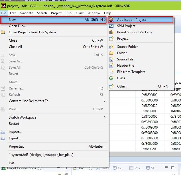
In SDK menu “New -> Application Project”, the establishment of a project APP
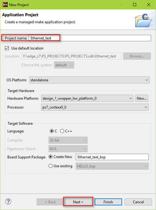
Enter Project Name as “Ethernet_test” and click next
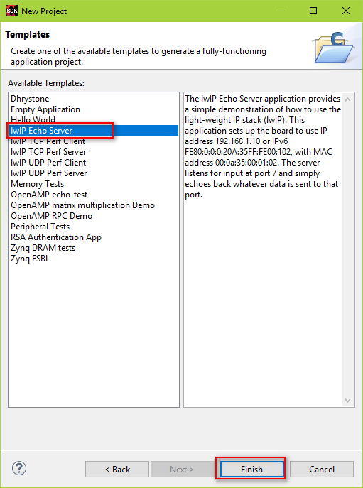
In the Template Selection window, select “lwIP Echo Server” and click “Finish”
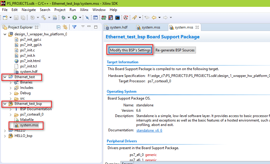
SDK creates “Ethernet_test” directory, “Ethernet_test_bsp” directory, you can find a lot of useful information in the “Ethernet_test_bsp” directory, where there are “BSP Documentation” contains a number of peripheral PS API description.
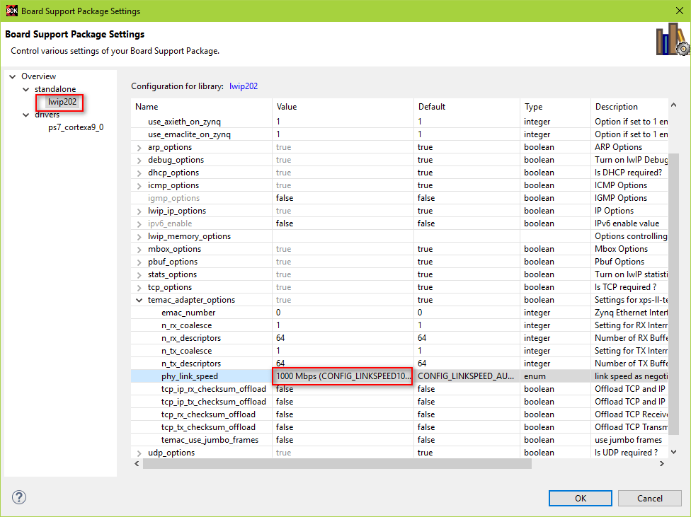
Next expand the “Ethernet_test_bsp” click on system.mss and select “modify this BSP’s Settings”
Next select lwip202 and expand temac_adapter_options. Then in the phy_link_speed parameter select 1000 Mbps (CONFIG_LINKSPEED1000) and click ok.
Now Connect the FPGA development board to the PC
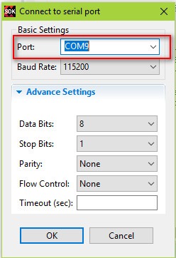
Downside of the SDK window you can see the SDK Terminal. Click on the + symbol.
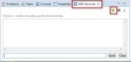
Select Com Port detected from FPGA USB UART. Also select Baud Rate as 115200 and click OK
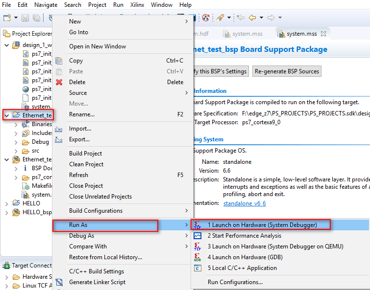
Right Click on the “Ehernet_test“ Application, click “Run As“ Launch on Hardware (system Debugger)
In the serial monitor of the screen the details of the connection will be displayed.
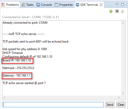
Connect your PC to your EDGE board using an Ethernet cable. If using a router, watch the UART console(given above picture) to find out the IP of the EDGE board echo server, and connect to that IP address. Setting up the connection as static is unnecessary.
In order to connect to the echo server directly from your computer, you must set up your Ethernet connection with a static IP address. To do this:
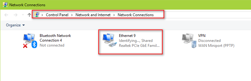
Find out the Ethernet connection to our board using the below path
Control panel => Network and Internet => Network Connections
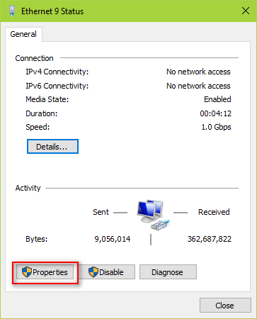
Click Properties.
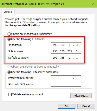
Select Internet Protocol Version 4 (TCP/IPv4) and click Properties.
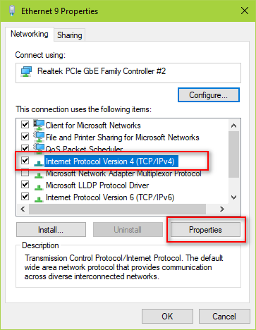
Click the Use the following IP address: bullet and type in an IP address “192.168.1.XX”, where XX is a value between 2 and 255, but not 10. This IP must not be the same as another already on your network. Make sure to click within the Subnet mask field to get the 255.255.255.0 mask to autofill. Click Ok and you will have a static IP address.
Click OK and close the Ethernet console.
You can see that the Ethernet is connected with the zynq board
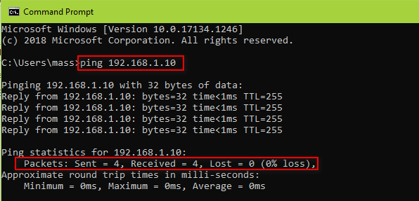
Now we can test the echo server by sending packets from our PC to the EDGE zynq board and looking at what gets sent back.
Ready to Ping Test
All Ethernet devices are required to respond to ping requests, so this is a very simple and easy test to perform using your computer. Just open a command window in your PC and type ping 192.168.1.10.
3. Memory Test
In SDK menu “New -> Application Project”, the establishment of a project APP
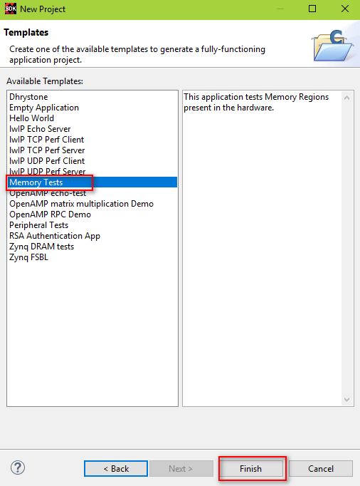
Enter Project name as “Memory_test”, click “Next”

In the Template Selection window, select “Memory_Tests” and click “Finish”
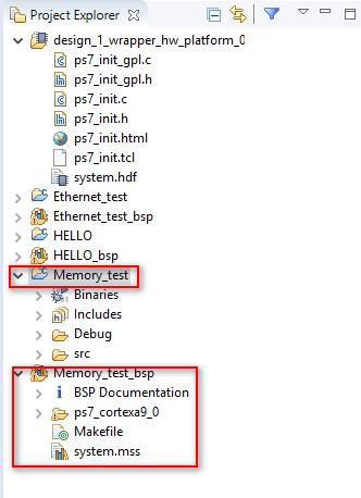
SDK creates “Memory_test” directory, “Memory_test _bsp” directory
Connect the FPGA development board to the PC
At the bottom of SDK window, select SDK Terminal and Click on the + symbol.

Select the COM port of the FPGA kit connected and select baud rate as 115200.

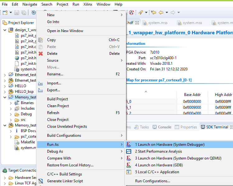
Right Click on the “Memory_test” Application and click “Run As“ Launch on Hardware (system Debugger)
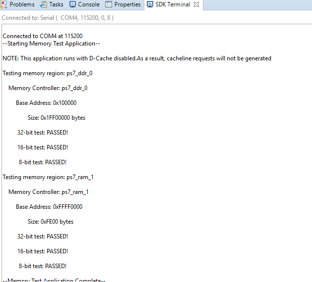
Both DDR3 memory and block RAM size and test will be displayed as shown below.
4. PS Push button and LED test
In SDK menu “New -> Application Project”, the establishment of a project APP
In the project name Enter “PS_pushbutton_LED” and click next.
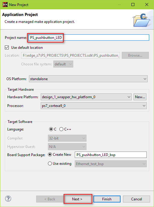
In the Template Selection window, select “Empty Application” and click “Finish”
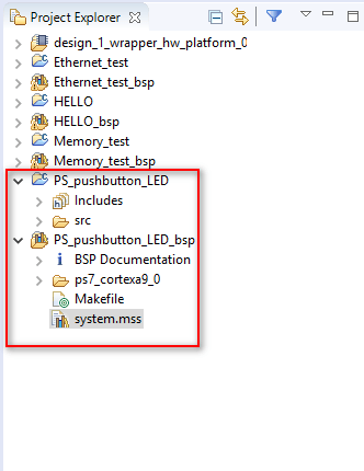
SDK creates an application with “PS_pushbutton_LED” directory, “PS_pushbutton_LED _bsp” directory, you can find a lot of useful information in the “PS_button_LED_bsp” directory, and where there are “BSP Documentation” contains a number of peripheral PS API descriptions.
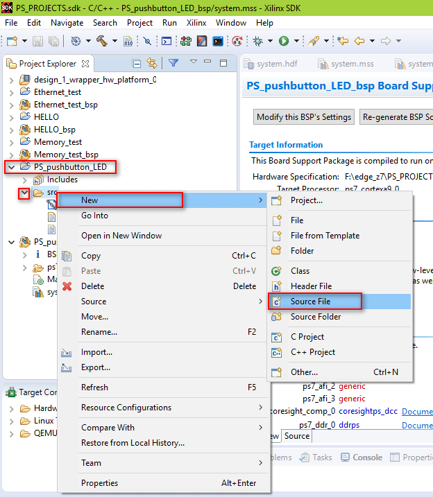
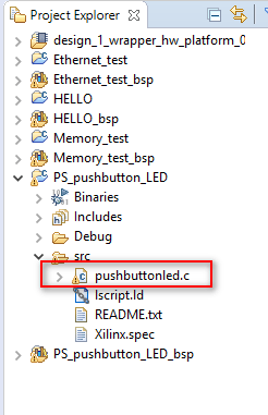
Right click PS_pushbutton_LED and click src New Source file
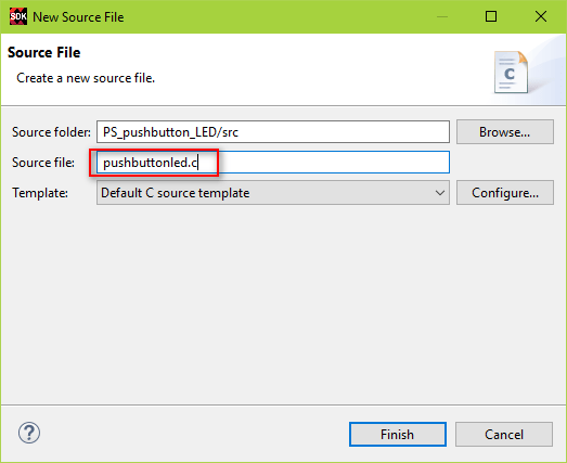
Give Source file as pushbuttonled.c and click Finish
Now the C file is created
Copy and Paste the below given C code on the created C file and save it.
#include <stdio.h>
#include “sleep.h”
#include “xgpiops.h”
#include “xparameters.h”
#define PS_LED_4 9
#define PS_BTN_4 0
int main()
{
int Status;
u32 data_reg;
XGpioPs_Config *ConfigPtr;
XGpioPs Gpio; /* The driver instance for GPIO Device. */
/* Initialize the GPIO driver.*/
ConfigPtr = XGpioPs_LookupConfig(XPAR_PS7_GPIO_0_DEVICE_ID);
Status = XGpioPs_CfgInitialize(&Gpio, ConfigPtr, ConfigPtr->BaseAddr);
if (Status != XST_SUCCESS) {
print(“cfg init err\n”);
return XST_FAILURE;
}
// LED4 configured as output
XGpioPs_SetDirectionPin(&Gpio, PS_LED_4, 1);
XGpioPs_SetOutputEnablePin(&Gpio, PS_LED_4, 1);
// BTN4 configured as input
XGpioPs_SetDirectionPin(&Gpio, PS_BTN_4, 0);
while (1)
{
Status = XGpioPs_ReadPin(&Gpio, PS_BTN_4);
printf(“Status = %i .”, Status);
if (Status == 1)
{
XGpioPs_WritePin(&Gpio, PS_LED_4, 1);
}
else
{
XGpioPs_WritePin(&Gpio, PS_LED_4, 0);
}
data_reg = XGpioPs_Read(&Gpio, 1);
sleep(1);
}
return 0;
}
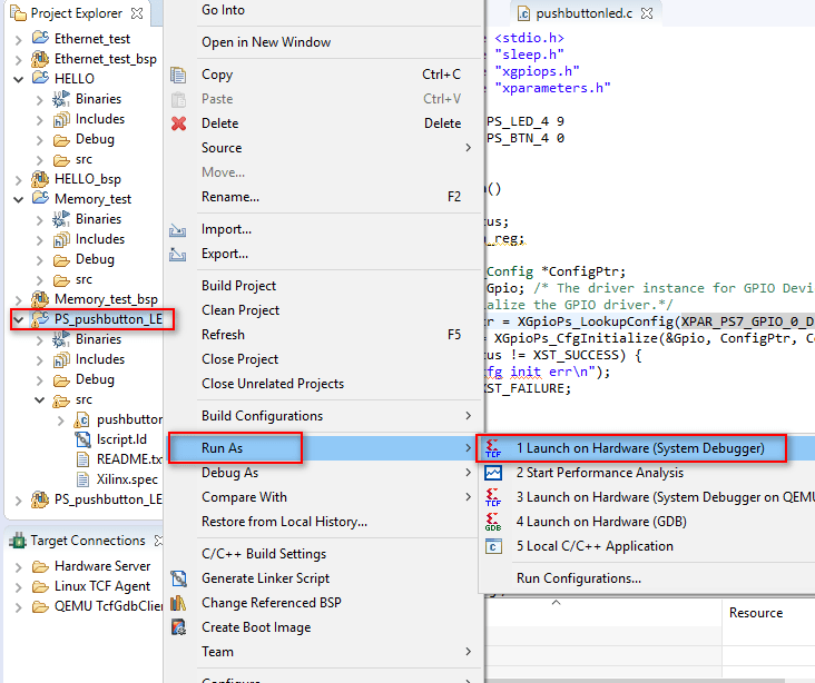
Connect the EDGE ZYNQ FPGA board to the PC. Right Click on the “PS_pushbutton_LED” and click “Run As“ Launch on Hardware (system Debugger)
In FPGA development board, Long Press the PS button and the LED will glow.
-
 EDGE ZYNQ SoC FPGA Development Board₹ 17,500