This Tutorial provides step by step procedure to create and run Microblaze design on EDGE Artix 7 FPGA Kit. First create hardware design and run software application on it. Entire system is configured on Artix 7 FPGA. The Peripheral test application demo outputs LED scrolling and Terminal output when soft Reset Switch is pressed.
Step 1: Open Vivado design Suite by selecting
Start > All Programs > Xilinx Design Tools > Vivado 2018.1 > Vivado 2018.1
Step 2: Click Create New Project and click next to open new project wizard.
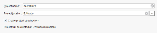
Step 3: Select Project directory and mention new project name.
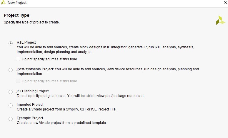
Step 4: Select RTL Project and check Do not specify sources at this time.
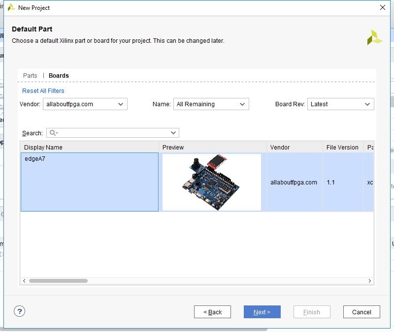
Step 5: This screen selects the part targeted by the project. edgeA7 Board Files installed to handle selecting complicated configuration settings. Select the Boards tab, then find and select the edgeA7 board from the list. Click Next.
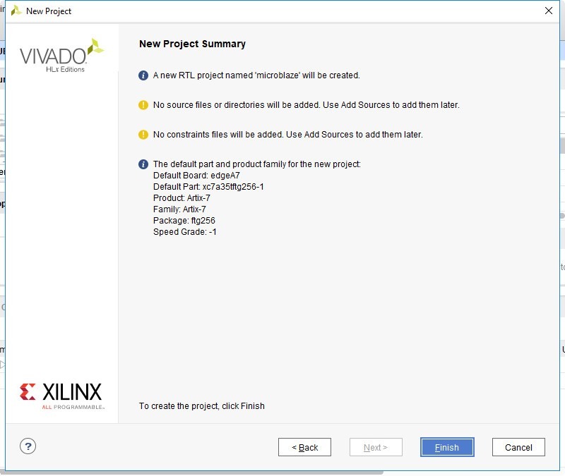
Step 6: Now the New Project summary display with project details selected.
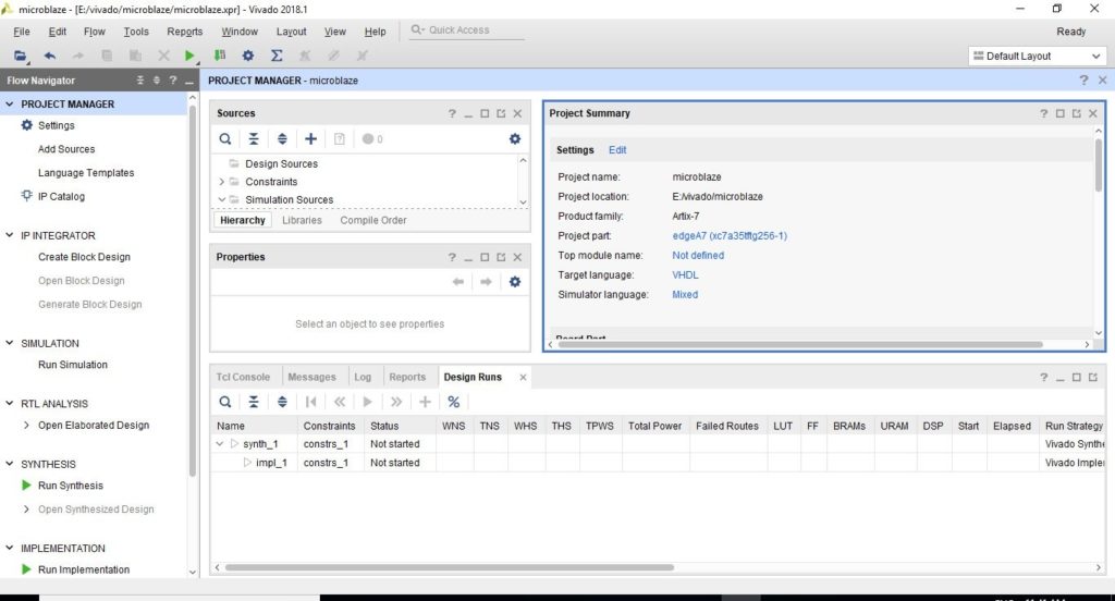
Step 7: Now the Vivado tool opens with Flow Navigator on left and on right Flow Navigator display the list of process involved from HDL input creation to bit file output generation. Project manager consist of Source, Workspace and Report Window.
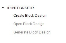
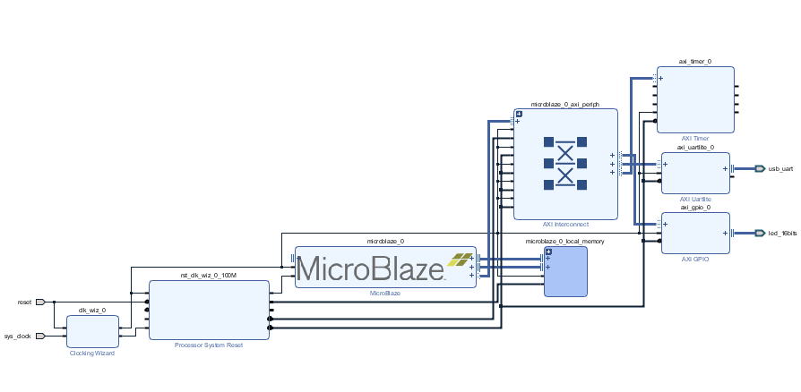
Step 8: Now design the microblaze project using IP integrator tool. To do this click on Create Block Design under IP Integrator in the flow navigator.
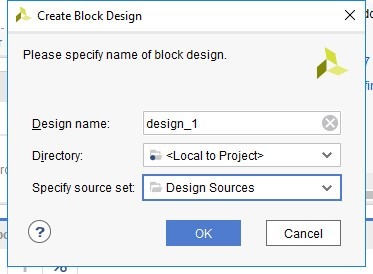
Step 9: Specify the design name and Leave both of the dropdown menus as their default shown below and click OK
Step 10: The IP integrator opens up in a new canvas. Now, right click on the canvas and select Add IP or click on the + symbol to add the IP blocks to the window.
Step 11: Click the +Add IP button and search for Microblaze.
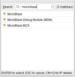
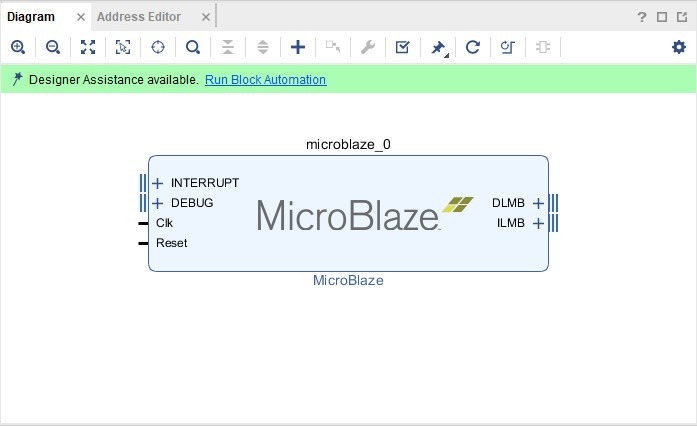
Step 12: Double click Microblaze to add it to your block design.
Step 13: Click the board tab which left to the block design console. We can see the board peripherals listed in the tab as shown in below.
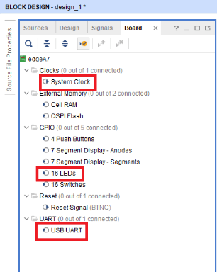
Step14: Click and drag the Highlighted peripheral such as System clock, 16 leds from GPIO and USB UART to the block design console.
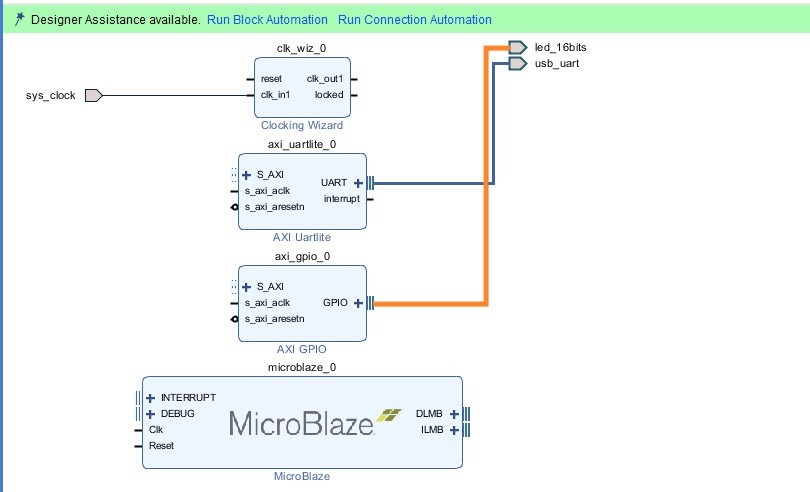
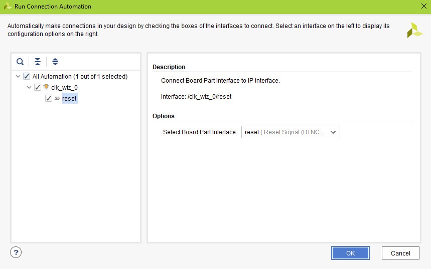
Step15: Click the Run connection automation in the green banner above. Click Ok. Then the reset tag will be added with clock wizard.
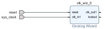
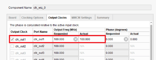
Step 16: Double click the Clocking Wizard block to customize it. Click on the Output Clocks tab and change clk_out1 to “100” MHz.
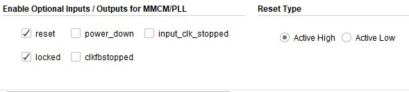
Step 16.1: Scroll down below and Set the Reset Type to Active Low
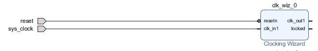
Step 17: Now the reset name is changed to resetn. Double click on the reset tag and make it is in active low condition and connect it with the clocking wizard.
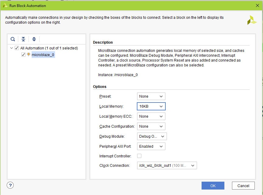
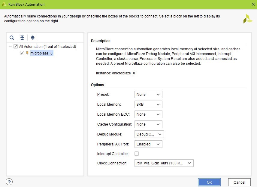
Step 18: Next, click on the Run block automation. It will pop up the Microblaze options. In that , leave the parameters as shown in below and click ok.
Step 19: Once you click the ok button, then the blocks will be connected automatically.
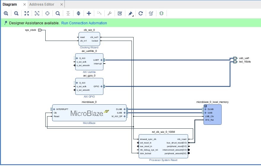
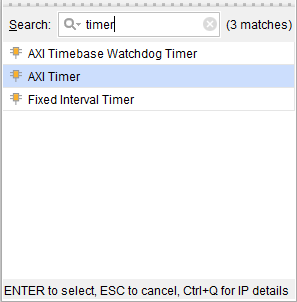
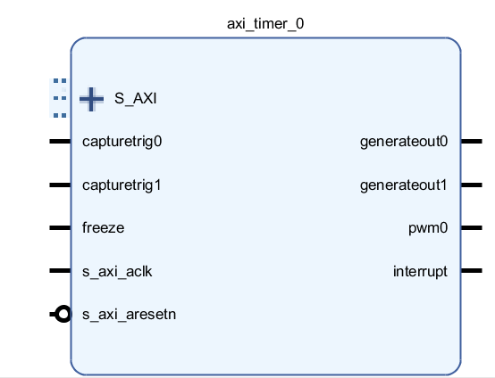
Step 20: Click the +Add IP button and search for Axi_timer. Add it to the design.
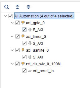
Step 21: Click on the Run connection automation that brings up new dialog box. Check the all boxes and click OK to confirm it.
Step 22: You will see the blocks will be connected together. Finally right click on the canvas and select regenerate layout. The blocks will be aligned correctly according to the input and output.
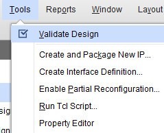
Step 23: Press F6 to Validate Design or Select Tools -> Validate Design . This will check for design and connection errors.
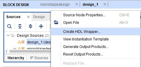
Step 24: In source window, right click on the design_1.bd and select Create HDL Wrapper.
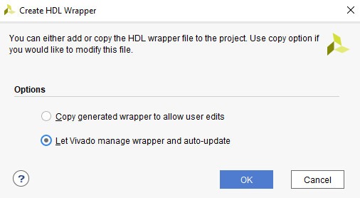
Step 25: Make sure Let Vivado manage wrapper and auto-update is selected and click OK.
This will create a top module in VHDL and will allow you to generate a bitstream.
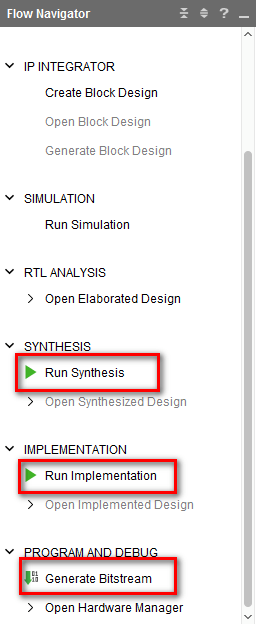
Step 26: Perform synthesis, Implementation and generate bitstream by click them one by one in Flow Navigator
After the bitstream has been generated, a message prompt will pop-up on the screen. You don’t have to open the Implemented Design for this demo. Just click Cancel.
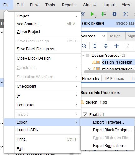
Step 27: Export the hardware design to SDK by choosing
File → Export → Export Hardware.
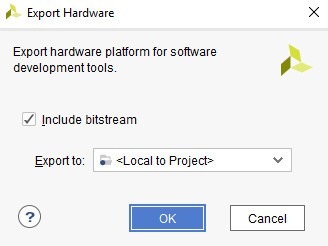
Step 28: In Export Hardware dialog box, select Include bitstream check box and Ensure that the Export to field is set to <Local to Project>. Then click OK button. This will export the hardware design with system wrapper for the Software Development Tool – Vivado SDK.
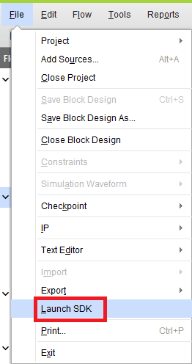
Step 29:Select File → Launch SDK
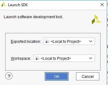
Step 30: This will populate the new dialog box. Leave both of the dropdown menus as their default Local to Project and click OK. This will open Xilinx SDK and import your hardware.
Step 31: SDK will launches in new window. It wil take some time to load
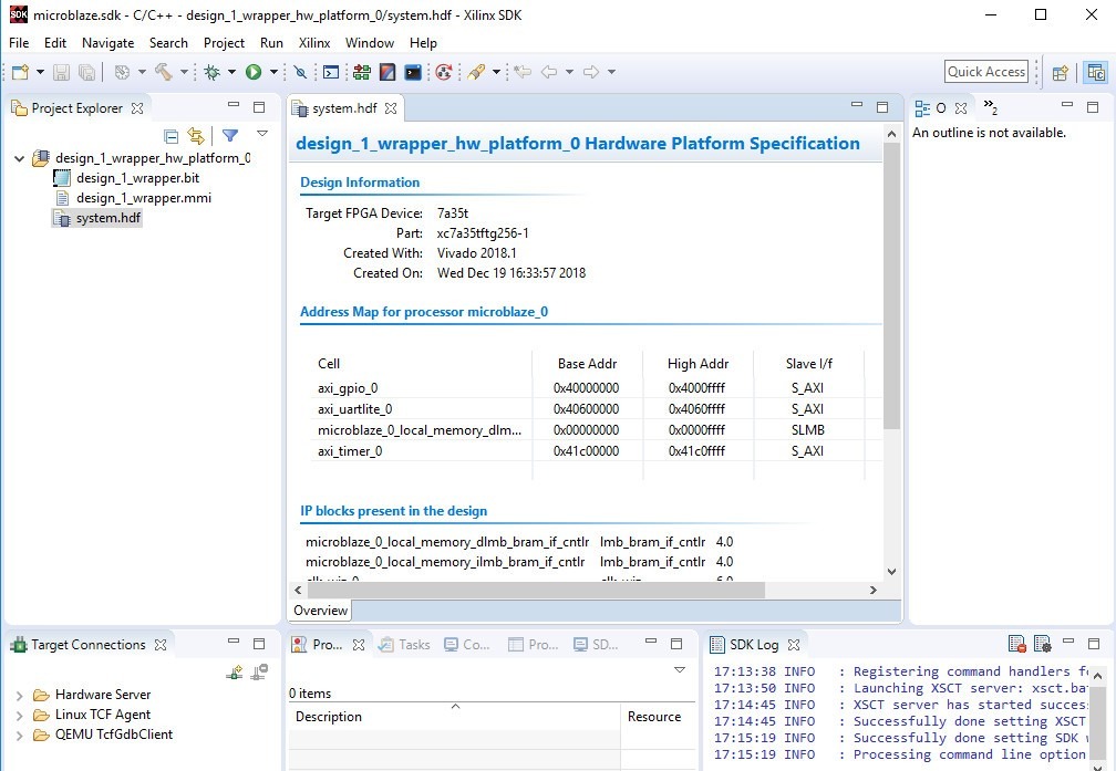
Step 32: The HW design specification and included IP blocks are displayed in the system.hdf file. Xilinx SDK is independent of Vivado, i.e. from this point, you can create your SW project in C/C++ on top of the exported HW design. If necessary, you can also launch SDK directly from the SDK folder created in the main Vivado Project directory.
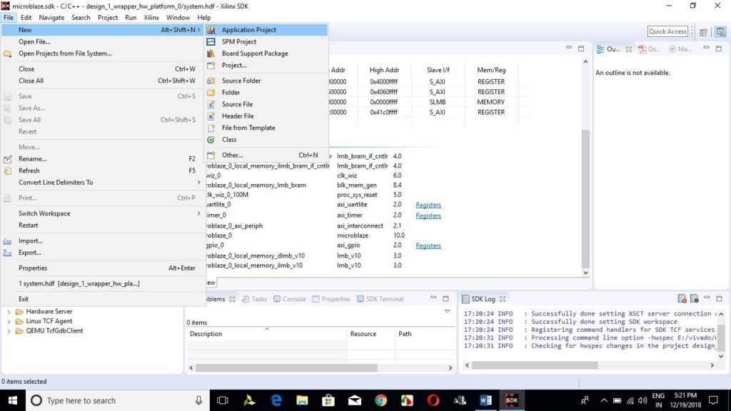
Step 33: Create a new application project by choosing
File→New→Appliction project
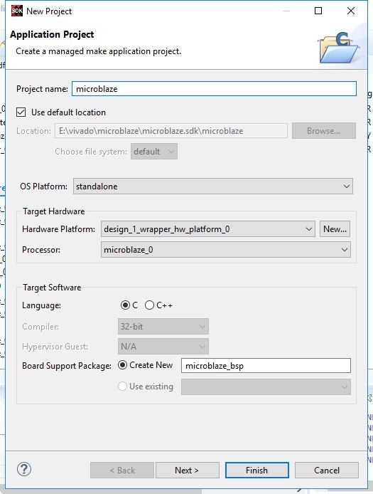
Step 34: Give a Project name and select C or C++ as target software. Click on Next to continue
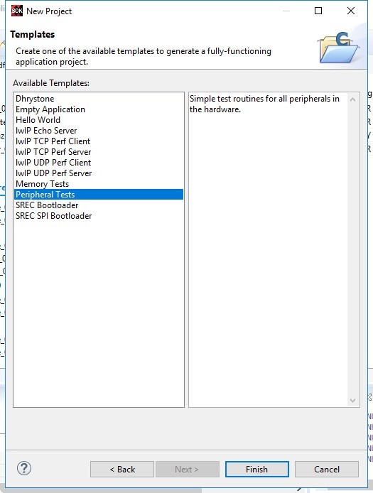
Step 35: Select Peripheral test from the list of templates and click Finish.
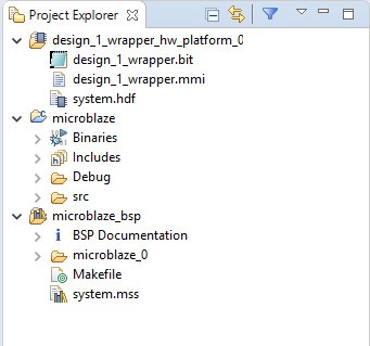
Step 36: Now, You will see two new folders in the Project Explorer panel.
- microblaze which contains all the binaries, .C and .H (Header) files
- microblaze_bsp which is the board support folder
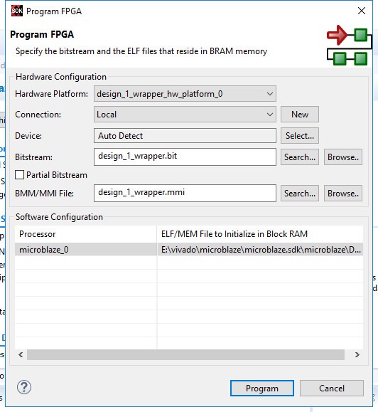
Step 37: Make sure that the FPGA board is connected with the host computer and board is turned on.
On the top toolbar, click the Program FPGA button.
Click Program to program your FPGA with your hardware design.
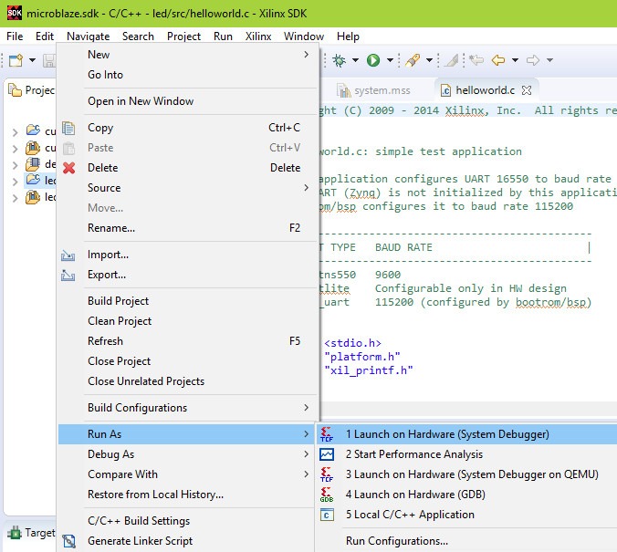
Program the Microblaze Processor choosing
Back in SDK, right click on the microblaze project> Run As… button. Select Launch on Hardware (System Debugger) and click OK.
Step 38: Finally the board is configured with program. Press the CPU RESET button in the Edge Artix 7 board, now you can examine the LED is blinking one by one according to the button press.
-
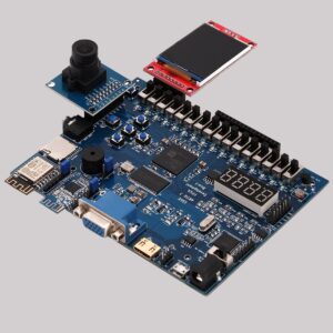 EDGE Artix 7 FPGA Development Board₹ 13,750