Altera FPGA Design Flow Tutorial

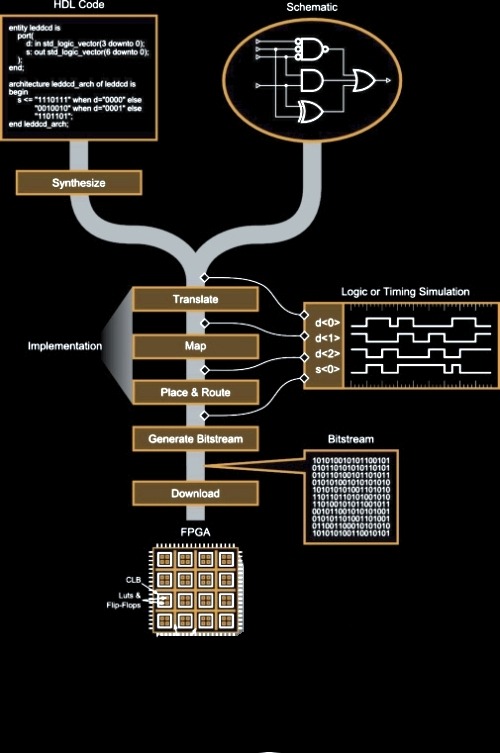
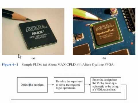
PLD FPGA Design flow (Sec 4-1)

This tutorial video describe Altera FPGA Design flow in simple explanation. This video tutorial was originally developed by Bill Kleitz.

FPGA Design Flow consist of

  • Design Entry
  • Synthesis
  • Implementation
  • Program FPGA

All those  procedure are clearly explained in the Altera FPGA Design flow Video Tutorial.


FPGA Design Flow

There are different techniques for design entry. Schematic based, Hardware Description Language and combination of both etc. . Selection of a method depends on the design and designer. If the designer wants to deal more with Hardware, then Schematic entry is the better choice. When the design is complex or the designer thinks the design in an algorithmic way then HDL is the better choice. Language based entry is faster but lag in performance and density.

Please Note: All the orders placed from 18th May 2025 to 27th June 2025 will be processed only by 1st July 2025. Sorry for the inconvenience. During this period you can contact us for technical support through email or WhatsApp.
This is default text for notification bar