Table of Contents
What is FPGA Configuration?
The FPGA is made of SRAM (Volatile Memory) so the data configured inside FPGA lost at power Off state. FPGA Configuration is the process of loading the FPGA chip with Configuration data through external devices during power On state.
The Method of Configuring FPGA Can be divided in to
- Master Mode
- Slave Mode
- JTAG Mode
Master Modes
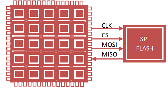
In the Master Mode the Configuration data is stored in external nonvolatile memories such us SPI FLASH, Parallel FLASH, PROM and so on. During configuration process the data is loaded in the FPGA Configurable Logic Blocks to operate as a specific application. The configuration clock is provided by FPGA in Master Mode operation.
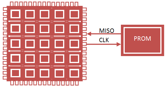
FPGA Configure through External PROM

FPGA Configure through SPI FLASH Memory
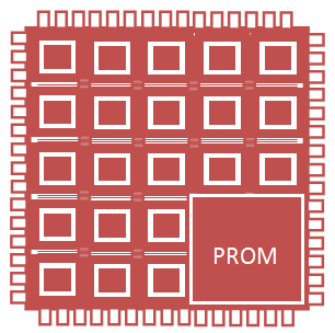
FPGA Configure through Internal FLASH
Slave Mode
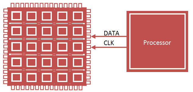
In Slave Mode, The entire configuration Process is controlled by External device. Those External device may be of processor, Microcontroller, and so on. The Configuration can performed serially or parallel method. The Clock input is supplied by the external device for Slave mode.
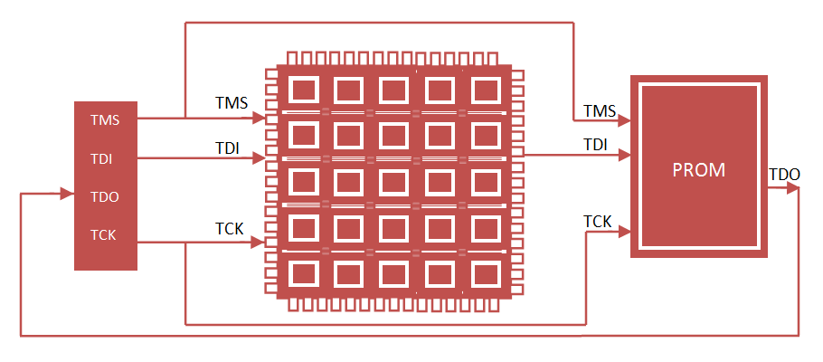
JTAG Connection
The four-wire JTAG interface is common on board testers and debugging hardware.FPGA mainly uses JTAG interface for prototype download and debugging. JTAG Consist of TCK, TMS, TDI and TDO lines for communication.
Thanks for the information. It’s very simple and concise.