All flip-flops can be divided into four basic types: SR, JK, D and T. They differ in the number of inputs and in the response invoked by different value of input signals.
Table of Contents
SR FlipFlop
A flip-flop circuit can be constructed from two NAND gates or two NOR gates. These flip-flops are shown in Figure. Each flip-flop has two outputs, Q and Q’, and two inputs, set and reset. This type of flip-flop is referred to as an SR flip-flop.
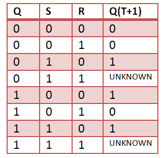
SR Flipflop truth table
VHDL Code for SR FlipFlop
library ieee;
use ieee. std_logic_1164.all;
use ieee. std_logic_arith.all;
use ieee. std_logic_unsigned.all;

entity SR_FF is
PORT( S,R,CLOCK: in std_logic;
Q, QBAR: out std_logic);
end SR_FF;

Architecture behavioral of SR_FF is
begin
PROCESS(CLOCK)
variable tmp: std_logic;
begin
if(CLOCK='1' and CLOCK'EVENT) then
if(S='0' and R='0')then
tmp:=tmp;
elsif(S='1' and R='1')then
tmp:='Z';
elsif(S='0' and R='1')then
tmp:='0';
else
tmp:='1';
end if;
end if;
Q <= tmp;
QBAR <= not tmp;
end PROCESS;
end behavioral;
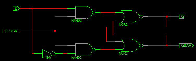
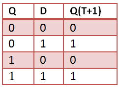
D FlipFlop
The D flip-flop shown in figure is a modification of the clocked SR flip-flop. The D input goes directly into the S input and the complement of the D input goes to the R input. The D input is sampled during the occurrence of a clock pulse. If it is 1, the flip-flop is switched to the set state (unless it was already set). If it is 0, the flip-flop switches to the clear state.
D Flipflop truth table
VHDL Code for D FlipFlop
library ieee;
use ieee. std_logic_1164.all;
use ieee. std_logic_arith.all;
use ieee. std_logic_unsigned.all;

entity D_FF is
PORT( D,CLOCK: in std_logic;
Q: out std_logic);
end D_FF;

architecture behavioral of D_FF is
begin
process(CLOCK)
begin
if(CLOCK='1' and CLOCK'EVENT) then
Q <= D;
end if;
end process;
end behavioral;
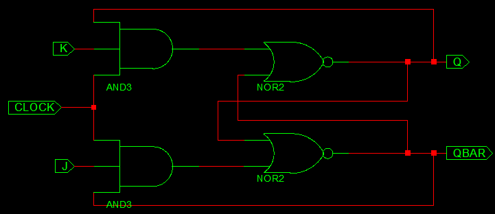
JK FlipFlop
A JK flip-flop is a refinement of the SR flip-flop in that the indeterminate state of the SR type is defined in the JK type. Inputs J and K behave like inputs S and R to set and clear the flip-flop (note that in a JK flip-flop, the letter J is for set and the letter K is for clear).
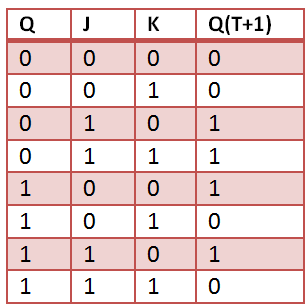
JK Flipflop truth table
VHDL Code for JK FlipFlop
library ieee;
use ieee. std_logic_1164.all;
use ieee. std_logic_arith.all;
use ieee. std_logic_unsigned.all;

entity JK_FF is
PORT( J,K,CLOCK: in std_logic;
Q, QB: out std_logic);
end JK_FF;

Architecture behavioral of JK_FF is
begin
PROCESS(CLOCK)
variable TMP: std_logic;
begin
if(CLOCK='1' and CLOCK'EVENT) then
if(J='0' and K='0')then
TMP:=TMP;
elsif(J='1' and K='1')then
TMP:= not TMP;
elsif(J='0' and K='1')then
TMP:='0';
else
TMP:='1';
end if;
end if;
Q<=TMP;
Q <=not TMP;
end PROCESS;
end behavioral;
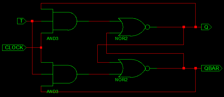
T FlipFlop
The T flip-flop is a single input version of the JK flip-flop. As shown in figure, the T flip-flop is obtained from the JK type if both inputs are tied together. The output of the T flip-flop “toggles” with each clock pulse.

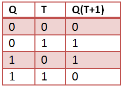
T Flipflop truth table
VHDL Code for T FlipFlop
library IEEE;
use IEEE.STD_LOGIC_1164.ALL;

entity T_FF is
port( T: in std_logic;
Clock: in std_logic;
Q: out std_logic);
end T_FF;

architecture Behavioral of T_FF is
signal tmp: std_logic;
begin
process (Clock)
begin
if Clock'event and Clock='1' then

if T='0' then
tmp <= tmp;
elsif T='1' then
tmp <= not (tmp);
end if;
end if;
end process;
Q <= tmp;
end Behavioral;
Kindly Correct your code . There are some minor mistakes .
I am not getting the correct values in the waveform with clk=1. Why is it happening?
Please, for the love of code, use indentations preferably with tabulations.
Can I know jk flip-flop using d flip-flop with test bench
nice
Easy and fast way to learn codes for flipflops
The presented solutions have many issues:
– The images don’t reflect the VHDL code, because the images show memory elements, which are state triggered (latch), whereas the VHDL code is edge triggered (flip-flop).
– Th D-flip-flop uses NAND gates, wheras all other flip-flops have and gates to “gate” the clock signal.
– Another error is that output Q in the JK implementation has a multiple driver problem.
– The D and T flip-flops have no QBAR output
– The truth table for the RS base-latch is wrong, because for R=S=1 the outputs Q and QBAR are not unknown. They have a value! It is unknown, what value will survive, while transitioning from R=S=1 (not allowed input combination) to R=S=0 (save value), because in most cases it’s not possible to predict if the transition goes the path S=0;R=1 or S=1;R=0. So for a very short time, between “not allowed” and “save” there will be either set or reset applied to the latch.
Regards
Patrick