Debounce
Push Button always got the mechanical property of bouncing state at micro sec.

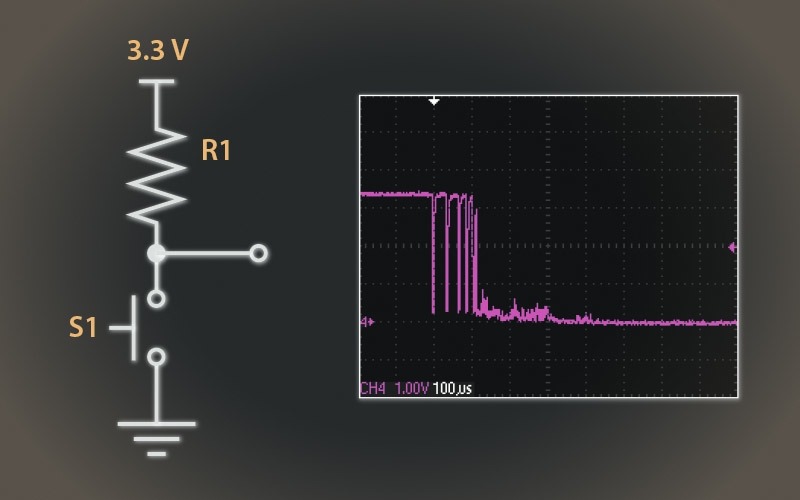
The above figure describes the debouncing output result, when the Push Button is pressed.
When you pull down the push button from high to low state. It bounce back to high and low few times before it settle at proper output. In order to avoid such bouncing state, we need to create debounce logic circuit.
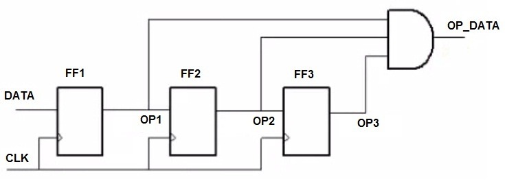
Debounce Logic Circuit
VHDL Code for Debounce Circuit in FPGA
library IEEE;
use IEEE.STD_LOGIC_1164.ALL;

entity VHDL_Code_Debounce is
Port (
DATA: in std_logic;
CLK : in std_logic;
OP_DATA : out std_logic);
end VHDL_Code_Debounce ;

architecture Behavioral of VHDL_Code_Debounce is

Signal OP1, OP2, OP3: std_logic;

begin

Process(CLK)

begin

If rising_edge(CLK) then

OP1 <= DATA;

OP2 <= OP1;

OP3 <= OP2;

end if;

end process;

OP_DATA <= OP1 and OP2 and OP3;

end Behavioral;
Above VHDL Code describes the method to avoid push Button debouncing. Instead of assigning the input data of push button to output, here 3 signals assigned OP1,OP2,OP3 and they all ANDed together and assigned to the output data.
If the FPGA clock is 50Mhz, the switch bouncing signal can last for longer than 3 (3 flip flop) * 20 ns (1/50Mhz) = 60 ns. That’s far form enough for mechanical switch.
It’s likely the CLK input is not the FPGA clock, but a clock signal that has been slowed down to a lower frequency using a clock divider.
Only one bit
Hi thank you for code but I have a question the data input could be n bits or only one bit?
Using 3 flip-flops is not enough. The bouncing signal from a button input can be seen for microseconds. Using a common 50, 100 or 200 MHz board clock as provided by all new FPGA development boards, results in > 100 flip-flips. So a debounce circuit should be realized with a counter to spare flip-flop and LUT resources. Moreover, the above mentioned solution does not address the input synchronization and meta-stability problem, which needs to be addressed for external asynchronous inputs like push buttons, too. Another problem with this solution is that the debounce behavior is not symmetric for low-high and high-low transitions.
why did you use 3 flip flip? how about 2 or 4? Could you explain, please!
3 Flipflop implementation makes the input stable for 3 clock cycle. If you increase the number of FlipFlop, it leads to more stable output. In case if you decrease, glitches increase.
good tech content
Thanks! keep coming…