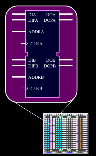
Block RAM:
- Xilinx FPGA Consist of 2 columns of memory called Block RAM or BRAM.
- It is a Dual port memory with separate Read/Write port.
- It can be configured as different data width 16Kx1, 8Kx8, 4Kx4 and so on.
- BRAM can be excellent for FIFO implementation.
- Multiple blocks can be cascaded to create still larger memory.
- The block RAM functions as dual or single-port memory.
- The maximum data path width of the block RAM is 18 bits.
Distributed RAM:
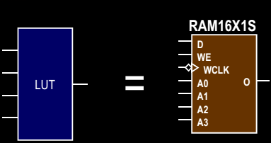
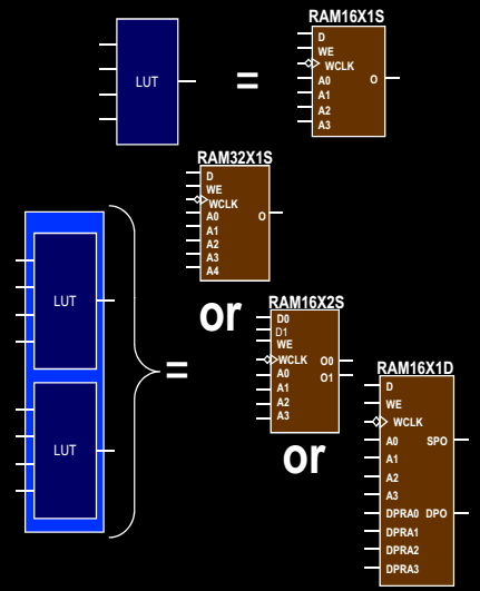
- CLB LUT configurable as Distributed RAM
- A LUT equals 16×1 RAM
- Implements Single and DualPorts
- Cascade LUTs to increase RAM size
- Synchronous write and Synchronous/Asynchronous read
https://www.xilinx.com/support/documentation/ip_documentation/bram_block.pdf
Maybe, you should note which FPGA(s) you are referring to, because these values are not true for e.g. Xilinx Virtex FPGAs.
– max datapath width of Virtex-5 BlockRAMs: 72 bits
– most (Xilinx) FPGAs have more than 2 BlockRAM columns
– distributed RAMs can also be used to build FIFOs and shift registers
Regards
Patrick