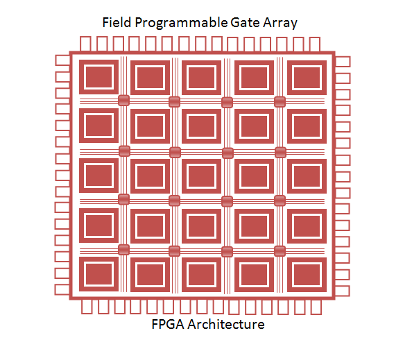
FPGA Configuration Tutorial

The FPGA is made of SRAM (Volatile Memory) so the data configured inside FPGA lost at power Off state. FPGA Configuration is the process of loading the FPGA chip with Configuration data through external devices during power On state.

FPGA Architecture

Field Programmable Gate Array

Field-programmable gate array (FPGA) is a device that has array of Configurable logic gates and can be programmed on-board through dedicated Joint Test Action Group (JTAG) or through any other serial/ Parallel non-volatile Memory. FPGA architecture are based on static random-access memory (SRAM) Volatile memory. The Data programmed inside the memory of an FPGA erase once the board powered off. In order to configure the data, external EEPROM is attached to FPGA.

FPGA Design Flow

There are different techniques for design entry. Schematic based, Hardware Description Language and combination of both etc. . Selection of a method depends on the design and designer. If the designer wants to deal more with Hardware, then Schematic entry is the better choice. When the design is complex or the designer thinks the design in an algorithmic way then HDL is the better choice. Language based entry is faster but lag in performance and density.

×

Chat with us for queries on the EDGE FPGA kit

×