VHDL Code for Binary to BCD Converter
By Support Team
/
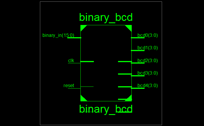
Binary to BCD Converter
Some times we need to display the output in a seven-segment display. For that purpose we will convert binary to BCD.
To translate from binary to BCD, we can employ the shift-and-add-3 algorithm:
Left-shift the (n-bit) binary number one bit.
If n shifts have taken place, the number has been fully expanded, so exit the algorithm.
If the binary value of any of the BCD columns is greater than or equal to 5, add 3.
Return to (1).
Read More
4 Replies
Block RAM and Distributed RAM in Xilinx FPGA
By Support Team
/
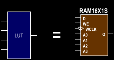
Block RAM:
Xilinx FPGA Consist of 2 columns of memory called Block RAM or BRAM.
It is a Dual port memory with separate Read/Write port.
It can be configured as different data width 16Kx1, 8Kx8, 4Kx4 and so on.
BRAM can be excellent for FIFO implementation.
Read More
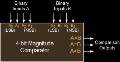
VHDL code for 4-bit binary comparator
By Support Team
/
Binary comparator compare two 4-bit binary number. It is also known as magnitude comparator and digital comparator. Analog form comparator is voltage comparator. The functionality of this comparator circuit is, It consist of 3 outputs Greater, Equal and Smaller. If inp-A is greater then inp-B then greater output is high, if both inp-A and inp-B are same then equal output is high, else smaller output is high.
Read More
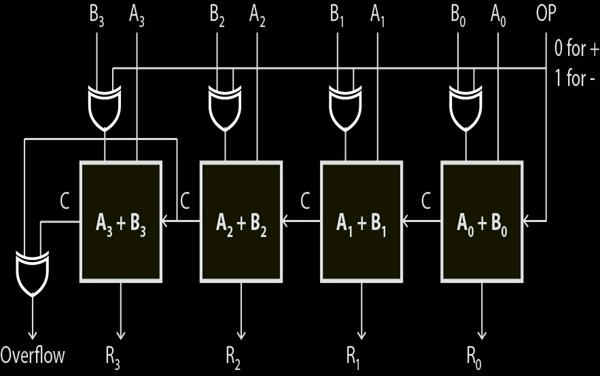
VHDL Code for 4-bit Adder / Subtractor
By Support Team
/
This example describes a two input 4-bit adder/subtractor design in VHDL. The design unit multiplexes add and subtract operations with an OP input. 0 input produce adder output and 1 input produce subtractor output.
Read More
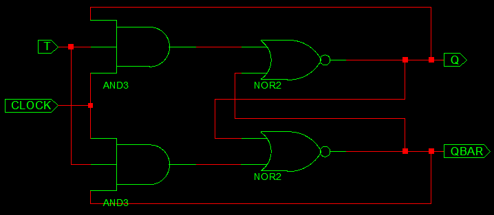
VHDL Code for Flipflop – D,JK,SR,T
By Support Team
/
All flip-flops can be divided into four basic types: SR, JK, D and T. They differ in the number of inputs and in the response invoked by different value of input signals.
SR FlipFlop
A flip-flop circuit can be constructed from two NAND gates or two NOR gates. These flip-flops are shown in Figure. Each flip-flop has two outputs, Q and Q', and two inputs, set and reset. This type of flip-flop is referred to as an SR flip-flop.
Read More
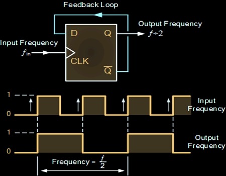
VHDL Code for Clock Divider (Frequency Divider)
By Support Team
/
Clock Divider is also known as frequency divider, which divides the input clock frequency and produce output clock. In our case let us take input frequency as 50MHz and divide the clock frequency to generate 1KHz output signal.
VHDL code consist of Clock and Reset input, divided clock as output. Count is a signal to generate delay, Tmp signal toggle itself when the count value reaches 25000. Output produce 1KHz clock frequency.
Reference count values to generate various clock frequency output
Read More
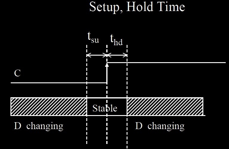
Setup Time and Hold Time in FPGA
By Support Team
/
Setup Time
The amount of time the synchronous input (D) must be stable before the active edge of the clock.
Hold Time
The amount of time the synchronous input (D) must be stable after the active edge of the clock.
Metastability
Read More

Digital Clock manager DCM in Xilinx FPGA
By Support Team
/
DCM provides clocking to all the resources of Xilinx FPGA with advanced feature. Digital Clock Manager DCM integrates advanced clocking capabilities to FPGA global clock distribution network.
It eliminates clock deskewing, Phase shifting, and also act as frequency synthesizer multiply/divide input clock.
Read More
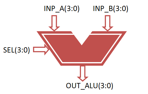
VHDL code for 4-bit ALU
By Support Team
/
ALU's comprise the combinational logic that implements logic operations such as AND, OR, NOT gate and arithmetic operations, such as Adder, Subtractor.
Functionally, the operation of typical ALU is represented as shown in diagram below,
Read More
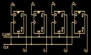
VHDL Code for 4-Bit Shift Register
By Support Team
/
Shift Register
VHDL Code for shift register can be categorised in serial in serial out shift register, serial in parallel out shift register, parallel in parallel out shift register and parallel in serial out shift register.
Read More
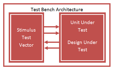
VHDL Testbench Tutorial
By Support Team
/
VHDL Testbench is important part of VHDL design to check the functionality of Design through simulation waveform. Testbench provide stimulus for design under test DUT or Unit Under Test UUT to check the output result.
A test bench is HDL code that allows you to provide a documented, repeatable set of stimuli that is portable across different simulators. Testbench consist of entity without any IO ports, Design instantiated as component, clock input, and various stimulus inputs.
Read More
FPGA Configuration Tutorial
By Support Team
/
The FPGA is made of SRAM (Volatile Memory) so the data configured inside FPGA lost at power Off state. FPGA Configuration is the process of loading the FPGA chip with Configuration data through external devices during power On state.
Read More
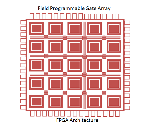
FPGA Architecture
By Support Team
/
Field-programmable gate array (FPGA) is a device that has array of Configurable logic gates and can be programmed on-board through dedicated Joint Test Action Group (JTAG) or through any other serial/ Parallel non-volatile Memory. FPGA architecture are based on static random-access memory (SRAM) Volatile memory. The Data programmed inside the memory of an FPGA erase once the board powered off. In order to configure the data, external EEPROM is attached to FPGA.
Read More
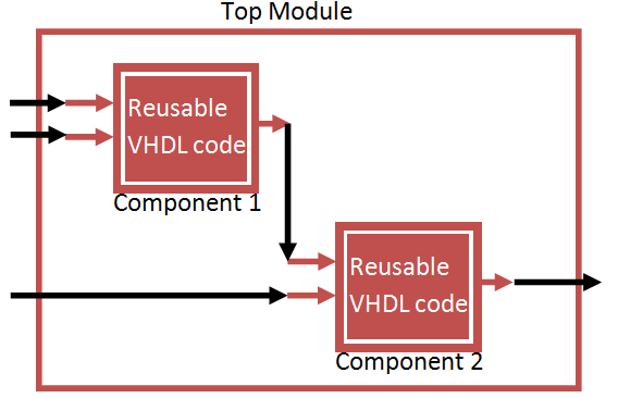
VHDL Component and Port Map Tutorial
By Support Team
/
Component is a reusable VHDL module which can be declared with in another digital logic circuit using Component declaration of the VHDL Code. This helps to implement hierarchical design at ease.
Instead of coding a complex design in single VHDL Code. we can divide the code in to sub modules as component and combine them using Port Map technique.
VHDL Port Map is the Process of mapping the input/ Output Ports of Component in Main Module.
Read More
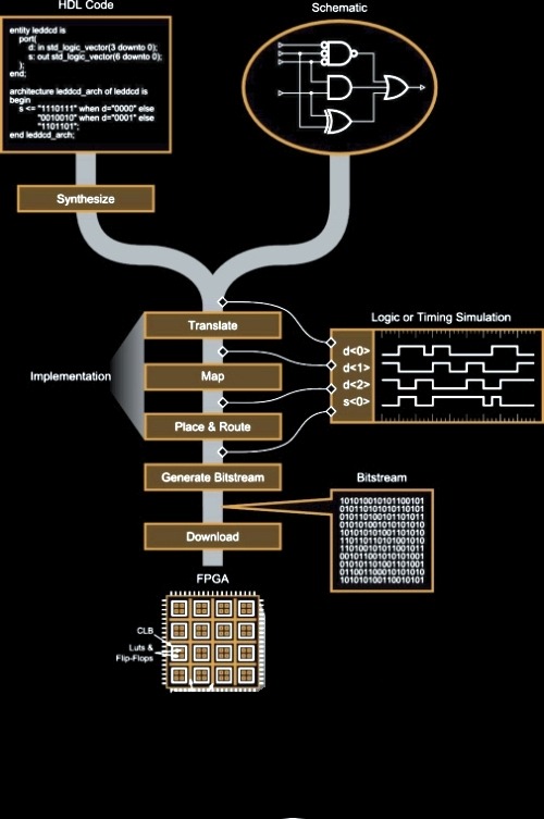
FPGA Design Flow
By Support Team
/
There are different techniques for design entry. Schematic based, Hardware Description Language and combination of both etc. . Selection of a method depends on the design and designer. If the designer wants to deal more with Hardware, then Schematic entry is the better choice. When the design is complex or the designer thinks the design in an algorithmic way then HDL is the better choice. Language based entry is faster but lag in performance and density.
Read More
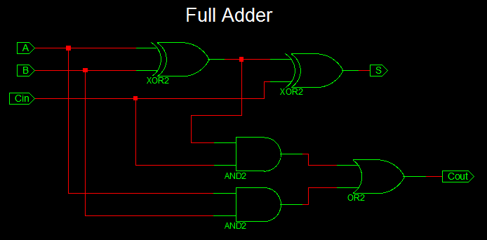
VHDL Code for Full Adder
By Support Team
/
The VHDL Code for full-adder circuit adds three one-bit binary numbers (A B Cin) and outputs two one-bit binary numbers, a sum (S) and a carry (Cout). Truth Table describes the functionality of full adder. sum(S) output is High when odd number of inputs are High. Cout is High, when two or more inputs are High. VHDL Code for full adder can also be constructed with 2 half adder Port mapping in to full adder.
Read More
VHDL Code for 4-Bit Binary Up Counter
By Support Team
/
The clock inputs of all the flip-flops are connected together and are triggered by the input pulses. Thus, all the flip-flops change state simultaneously (in parallel).
Read More
-
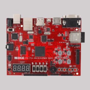 EDGE ZYNQ SoC FPGA Development Board₹ 17,500
 -
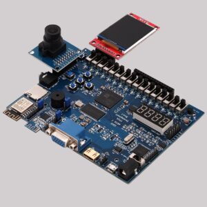 EDGE Artix 7 FPGA Development Board₹ 13,750
 -
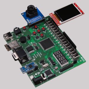 EDGE Spartan 6 FPGA Development Board₹ 8,500